Portable capacitance tomography measuring device

A technology of electrical capacitance tomography and measuring equipment, which is applied in the direction of material capacitance, etc., can solve the problems of ECT system not having portability, linear power supply volume, and heavy weight, etc., and achieves the advantages of easy function expansion, low power consumption, and improved stability Effect

Active Publication Date: 2019-06-18
BEIHANG UNIV
10 Cites 4 Cited by

AI-Extracted Technical Summary

Problems solved by technology

However, existing electrical capacitance tomography measurement systems are limited by power consumption and require an e...

Abstract

The invention relates to a portable capacitance tomography measuring device. The device is characterized by mainly comprising five parts, including a power module (1), a clock and control module (2),a signal generation module (3), a capacitance measurement module (4) and a data acquisition and transmission module (5), wherein the modules of the circuit are uniformly connected with a standard businterface and are powered and communicated through an industry standard bus, each module includes a corresponding simulation circuit and a digital logic circuit, the power module (1) is composed of alithium battery and a power management circuit, the clock and control module (2) is composed of a crystal oscillator circuit, a control clock and a switch circuit, the signal generation module (3) iscomposed of a lookup table register and a digital-to-analog conversion circuit, the capacitance measurement module (4) is composed of a current-voltage conversion circuit and a digital demodulator, and the data acquisition and transmission module (5) is composed of an on-chip storage circuit and a universal serial bus communication circuit.

Application Domain

Material capacitance

Technology Topic

TomographyDigital logic circuits +13

Image

  • Portable capacitance tomography measuring device
  • Portable capacitance tomography measuring device
  • Portable capacitance tomography measuring device

Examples

  • Experimental program(1)

Example Embodiment

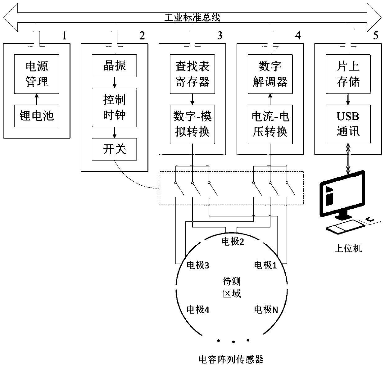
[0015] Such as figure 1 As shown, the present invention mainly includes five parts: power module (1), clock and control module (2), signal generation module (3), capacitance measurement module (4) and data acquisition and transmission module (5); Each module is uniformly connected to the standard bus interface, power supply and communication through the industry standard bus; each module includes the corresponding analog circuit and digital logic circuit; the power module (1) is composed of lithium battery and power management circuit; clock and control module ( 2) Composed of crystal oscillator circuit, control clock and switch circuit; signal generation module (3) is composed of look-up table register and digital-to-analog conversion circuit; capacitance measurement module (4) is composed of current-voltage conversion circuit and digital demodulator; The data acquisition and transmission module (5) is composed of an on-chip storage circuit and a universal serial bus communication circuit. The specific implementation is as follows:
[0016] 1) Use 5 lithium batteries in parallel as the power supply, use the voltage regulator chip to output 3.3V, 5V, 12V and other voltages, and connect to the voltage pins of the CPCI bus;
[0017] 2) Choose 40MHz passive crystal oscillator and complex programmable logic device (CPLD) chip, divide the 40MHz clock signal into 100kHz~1MHz control signal, such as figure 2 The clock signal and control signal in
[0018] 3) Edit the look-up table of 40-400 sinusoidal signals with a timing value of one period in the register of the CPLD chip, and input the digital-analog conversion circuit under the trigger of a 40MHz clock signal to form an excitation signal of 100kHz-1MHz, such as figure 2 The sequence value and excitation signal of the look-up table in
[0019] 4) When the control signal is high, it enters the capacitance measurement period, when the control signal is low, it enters the switch switching period;
[0020] 5) In each switch switching cycle, the switch changes its off state, switches the excitation signal or the electrode of the measurement circuit, and traverses the measurement capacitor array in turn;
[0021] 6) The current-voltage conversion circuit converts the current on the measuring electrode into a voltage signal, and the analog-digital conversion circuit converts the analog voltage signal into a digital voltage signal, which is input to a digital demodulator;
[0022] 7) The shaping and demodulation of the measurement signal is realized on the complex programmable logic device (CPLD) chip, the principle is as follows:
[0023] ①Assuming that the discrete signal collected by the analog-digital conversion circuit triggered by a 40MHz clock signal is
[0024]
[0025] Among them, A is the output amplitude of the sinusoidal voltage signal of the analog-digital conversion circuit, A r Is the output value of the ground reference voltage, n is the sampling point number, f is the signal frequency, f s Is the sampling frequency, Is the signal phase.
[0026] ② Convert the discrete signal V(n) into the deviation from the ground reference voltage:
[0027]
[0028] ③When the control signal is at high level and enters the capacitance measurement period, under the trigger of the clock signal, add a signal period to d(n) to obtain:
[0029]
[0030] ④ Obtain the amplitude of the voltage signal to be measured, that is, the product of the fixed coefficient and the capacitance value to be measured:
[0031]
[0032] 8) When the falling edge of the control signal is detected, write the calculated capacitance value into the on-chip memory chip;
[0033] 9) After the capacitance array measurement is completed, charge the lithium battery, connect the circuit of the present invention to the upper computer through the universal serial bus communication interface, use the universal serial bus of the upper computer to supply power, and read the data in the memory chip.

PUM

no PUM

Description & Claims & Application Information

We can also present the details of the Description, Claims and Application information to help users get a comprehensive understanding of the technical details of the patent, such as background art, summary of invention, brief description of drawings, description of embodiments, and other original content. On the other hand, users can also determine the specific scope of protection of the technology through the list of claims; as well as understand the changes in the life cycle of the technology with the presentation of the patent timeline. Login to view more.

Similar technology patents

Semiconductor device including capacitorless ram

ActiveUS20090310431A1reduce power consumptionretention time be lengthen
Owner:LONGITUDE LICENSING LTD

Efficient route update protocol for wireless sensor network

InactiveUS20050157698A1minimize power consumption differencereduce power consumption
Owner:SAMSUNG ELECTRONICS CO LTD +1

Lighted bollard

InactiveUS20060109667A1reduce power consumption
Owner:LEADER MFG

Classification and recommendation of technical efficacy words

  • Improve stability
  • reduce power consumption

Electrode array for use in medical stimulation and methods thereof

InactiveUS20050038489A1reduce power consumptionincrease battery life
Owner:CASE WESTERN RESERVE UNIV

Method of reselecting a cell based on priorities

ActiveUS20090181676A1ensure quality of servicereduce power consumption
Owner:LG ELECTRONICS INC

Organic light-emitting devices with mixed electron transport materials

InactiveUS20060204784A1good luminance efficiency and stabilityreduce power consumption
Owner:EASTMAN KODAK CO
Why Eureka
Try Eureka