Micron panchromatic QLED array device based on deep silicon etching template quantum dot transfer process and preparation method of micron panchromatic QLED array device

A technology of deep silicon etching and quantum dots, which is used in electric solid devices, semiconductor devices, electrical components, etc., can solve the problems of difficulty in filling and transferring multi-color quantum dots, and complicated processes.

Active Publication Date: 2019-06-25
NANJING UNIV
View PDF4 Cites 9 Cited by
  • Summary
  • Abstract
  • Description
  • Claims
  • Application Information

AI Technical Summary

Problems solved by technology

However, ordinary Micro-LEDs still have great difficulties in realizing multi-color display, such as complicated process, and it is difficult to realize the filling and transfer of multi-color quantum dots

Method used


Image

  • Micron panchromatic QLED array device based on deep silicon etching template quantum dot transfer process and preparation method of micron panchromatic QLED array device
  • Micron panchromatic QLED array device based on deep silicon etching template quantum dot transfer process and preparation method of micron panchromatic QLED array device
  • Micron panchromatic QLED array device based on deep silicon etching template quantum dot transfer process and preparation method of micron panchromatic QLED array device

Examples


Embodiment 1

[0084] Example 1 Micron full-color QLED array device based on deep silicon etching template quantum dot transfer process

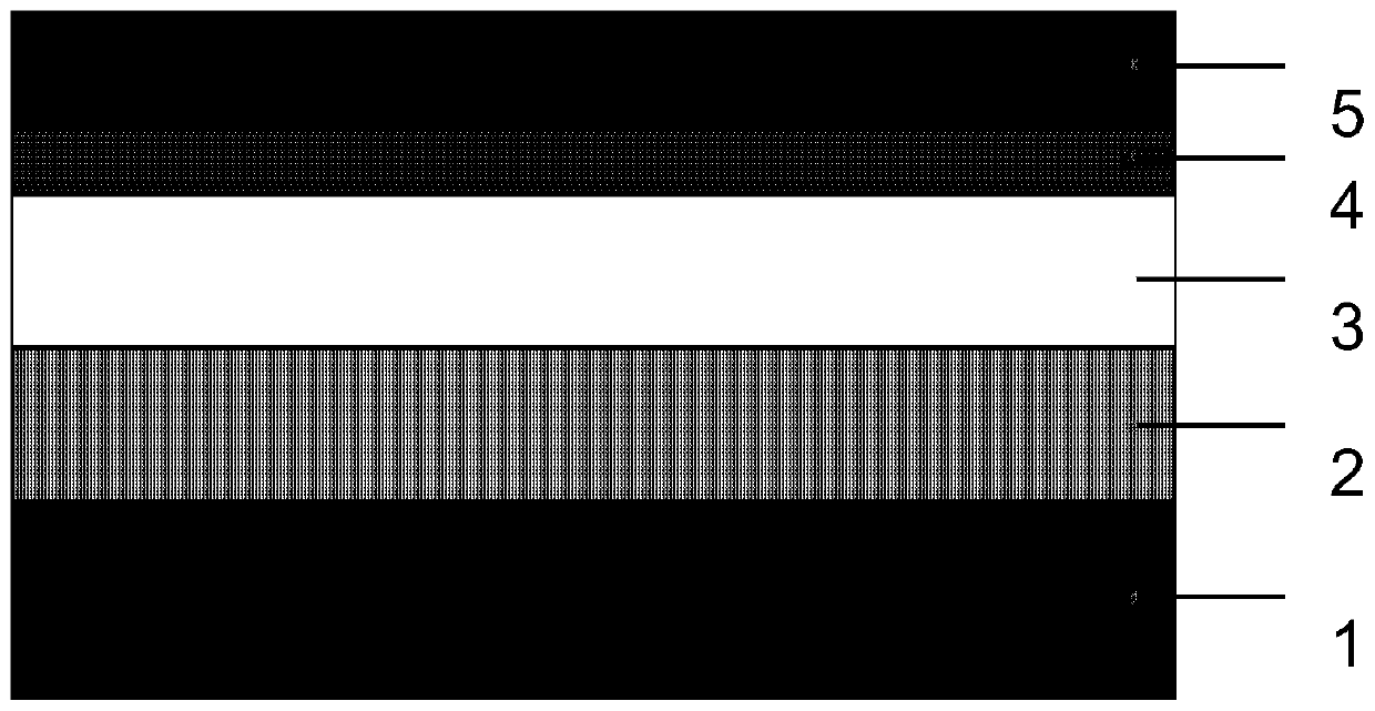
[0085] The epitaxial wafer structure selected for the substrate material in this implementation case is as follows figure 1 As shown, a standard blue LED epitaxial wafer with a p-n structure includes a sapphire substrate 1; a gallium nitride buffer layer 2 grown on the sapphire substrate; an n-type gallium nitride layer 3 grown on the buffer layer; A quantum well active layer 4 on the quantum well active layer; a p-type gallium nitride layer 5 grown on the quantum well active layer.

[0086] The specific preparation method of the Micro-LED array device is as follows:

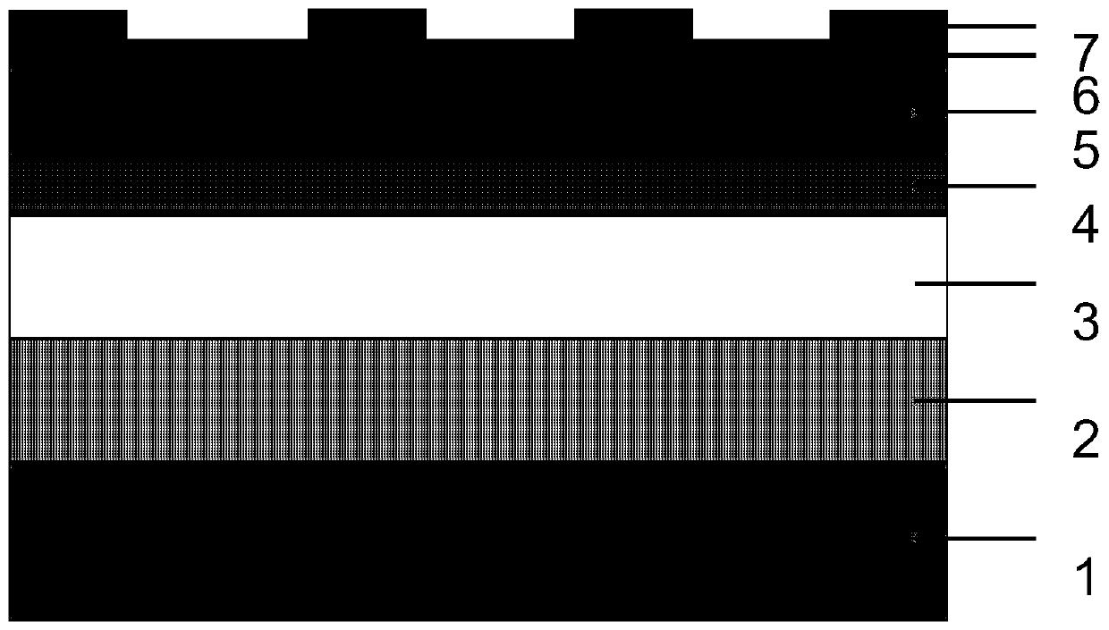
[0087] (1) if figure 2 As shown, using plasma-enhanced chemical vapor deposition (PECVD) technology, in In x Ga 1-x Evaporation of a layer of 150nm thick SiO on N / GaN quantum well blue LED epitaxial wafer 2 Dielectric layer 6, PECVD grown SiO 2 The way is to pass 5% SiH into the react...

Embodiment 2

[0108] Example 2 Micron full-color QLED array device based on deep silicon etching template quantum dot transfer process

[0109] The epitaxial wafer structure selected for the substrate material in this implementation case is as follows figure 1 As shown, a standard blue LED epitaxial wafer with a p-n structure includes a sapphire substrate 1; a gallium nitride buffer layer 2 grown on the sapphire substrate; an n-type gallium nitride layer 3 grown on the buffer layer; A quantum well active layer 4 on the quantum well active layer; a p-type gallium nitride layer 5 grown on the quantum well active layer.

[0110] The specific preparation method of the Micro-LED array device is as follows:

[0111] (1) if figure 2 As shown, using plasma-enhanced chemical vapor deposition (PECVD) technology, in In x Ga 1-x Evaporation of a layer of 200nm thick SiO on N / GaN quantum well blue LED epitaxial wafer 2 Dielectric layer 6, PECVD grown SiO 2 The way is to pass 5% SiH into the react...

Embodiment 3

[0132] Example 3 Micron full-color QLED array device based on deep silicon etching template quantum dot transfer process

[0133] The epitaxial wafer structure selected for the substrate material in this implementation case is as follows figure 1 As shown, a standard blue LED epitaxial wafer with a p-n structure includes a sapphire substrate 1; a gallium nitride buffer layer 2 grown on the sapphire substrate; an n-type gallium nitride layer 3 grown on the buffer layer; A quantum well active layer 4 on the quantum well active layer; a p-type gallium nitride layer 5 grown on the quantum well active layer.

[0134] The specific preparation method of the Micro-LED array device is as follows:

[0135] (1) if figure 2 As shown, using plasma-enhanced chemical vapor deposition (PECVD) technology, in In x Ga 1-x Evaporation of a layer of 250nm thick SiO on N / GaN quantum well blue LED epitaxial wafer 2 Dielectric layer 6, PECVD grown SiO 2 The way is to pass 5% SiH into the react...


PUM


Abstract

The invention discloses a micron panchromatic QLED array device based on a deep silicon etching template quantum dot transfer technology. An array-type square mesa structure penetrating through a p-type GaN layer, a quantum well active layer and a deep-to-n-type GaN layer is arranged on a blue light LED epitaxial wafer, and micron holes are formed in the array-type square mesa structure through etching. Every 2*2 mesa structures form an RGB pixel unit, and the four micrometer holes are filled with red light quantum dots, green light quantum dots, yellow light quantum dots and blue light quantum dots. The micro-holes are etched the silicon wafer through by the deep silicon etching technology, the micro-holes in the silicon waver are aligned with the quantum dot filling areas on the Micro-LED, and the quantum dots are spin-coated into the Micro-LED. The invention also discloses a preparation method thereof. Three different deep silicon etching mask plates can complete spin coating of green light, red light and yellow light quantum dots in the Micro-LED, thereby achieving the panchromatic display of RGB pixel units, and forming a QLED array device.

Description

technical field [0001] The invention relates to a micron full-color QLED array device based on a deep silicon etching template quantum dot transfer process and a preparation method thereof, belonging to the technical field of semiconductor lighting and display. Background technique [0002] As a lighting source widely used at present, light-emitting diodes have the advantages of high efficiency, good impact and shock resistance, high reliability, long life, and environmental protection compared with traditional lighting sources. Group III nitride materials are direct bandgap semiconductors, and their bandgap covers the infrared-visible-ultraviolet band, which has become the main material used in the current solid-state high-efficiency lighting technology. Compared with traditional incandescent lighting, LED light source has the advantages of using low-voltage power supply, less energy consumption, strong applicability, high stability, short response time, no pollution to the...

Claims


Application Information

Patent Timeline
Patent Type & Authority Applications(China)
IPC IPC(8): H01L27/15H01L33/50H01L33/44
CPCH01L27/156H01L33/502H01L33/007H01L33/0095H01L33/32H01L33/40
Inventor 刘斌蒋迪余俊驰王轩陶涛潘丹峰谢自力周玉刚陈敦军修向前张荣
Owner NANJING UNIV
Why Eureka
Try Eureka