Filament mechanism-based small-area electrode resistive random access memory and preparation method thereof

A resistive variable memory, small-area technology, applied in the direction of electrical components, etc., can solve the problems of enhancing the uncertainty of resistive variable behavior, the uncontrollable position of filament formation, and the inability to use multiple times, so as to reduce fluctuations and optimize devices , to achieve the effect of control

Pending Publication Date: 2019-07-05
HENAN UNIVERSITY
View PDF8 Cites 3 Cited by
  • Summary
  • Abstract
  • Description
  • Claims
  • Application Information

AI Technical Summary

Problems solved by technology

[0008] However, in the prior art, the method of guiding the formation of electrode filaments to reduce the effective electrode area still has the following limitations. For example, the limitation of electrode material selection in background technology 3 requires not only the electrode material and resistive layer for forming electrode filaments Ohmic contact is naturally formed when in contact, and Al is also required to pass through SiO 2 Layer defects penetrate into the Si layer to make Si dissolve in Al to form electrode fi...

Method used


Image

  • Filament mechanism-based small-area electrode resistive random access memory and preparation method thereof
  • Filament mechanism-based small-area electrode resistive random access memory and preparation method thereof
  • Filament mechanism-based small-area electrode resistive random access memory and preparation method thereof

Examples


Embodiment 1

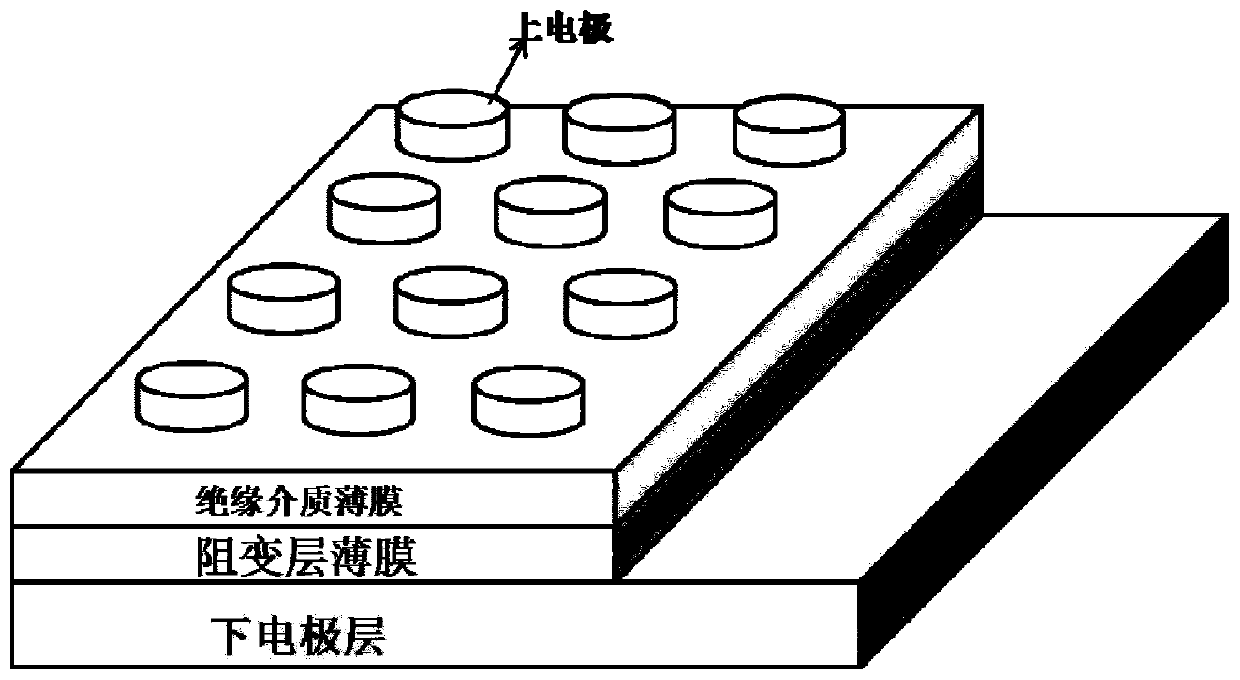
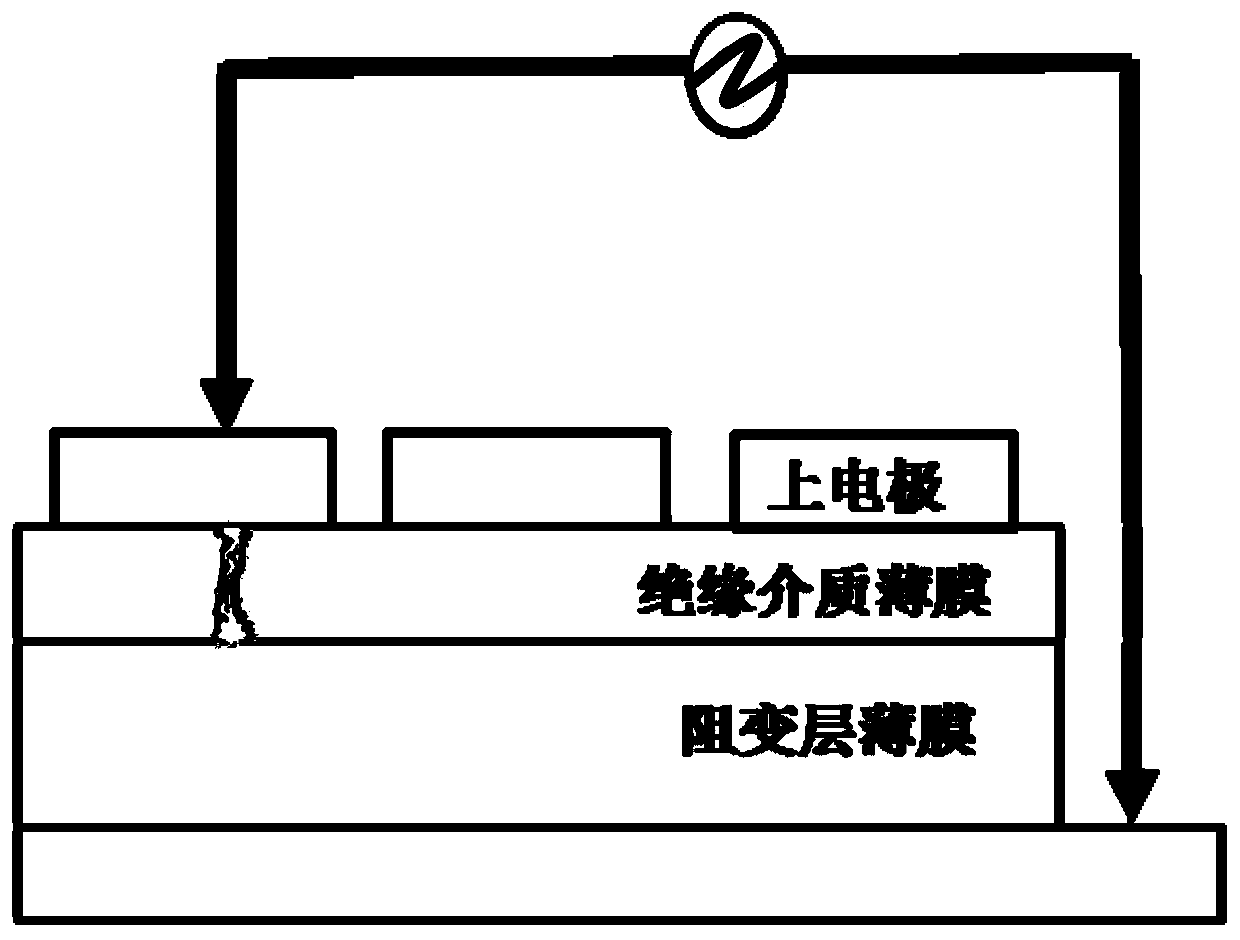
[0031] A copper sheet is selected as the lower electrode, and a boron nitride film is deposited on it as a resistive layer by magnetron sputtering, with a thickness of about 50nm; a plurality of aluminum metal upper electrodes with a thickness of about 150nm are deposited by using a mask plate through PVD process . The electrical characteristics are tested by a semiconductor parameter analyzer. The device is a unipolar resistive memory device that can realize unipolar operation. Its Reset voltage is concentrated around 1.3V, and the distribution range is plus or minus 0.3V, that is, Reset The voltage distribution is 1-1.6V, and the concentration is around 1.3V.

[0032] Under the same preparation process conditions, a 5nm aluminum oxide insulating layer is prepared between the upper electrode and the resistive switch layer by thermal oxidation process. The device is a unipolar resistive switch memory device, which can realize unipolar operation. Its Reset voltage is concentra...

Embodiment 2

[0034] The Pt substrate is selected as the lower electrode, and N-type TiO with a thickness of about 70 nm is grown on it by ion beam assisted reactive sputtering. 2 thin film, on TiO 2 A P-type NiO film with a thickness of about 70 nm was prepared on the film by ion beam-assisted reactive sputtering, and TiO 2 / NiO stacked structure as the resistive layer; through the ion sputtering process, through the mask plate, in the TiO 2 Au electrodes with a thickness of 30 nm were prepared on the stacked structure of NiO / NiO. The electrical characteristics are tested by a semiconductor parameter analyzer. The device is a unipolar resistive memory device that can realize unipolar operation. Its Reset voltage is concentrated around 1.5V, and the distribution range is plus or minus 0.5V, that is, Reset The voltage distribution is 1-2V, and the concentration is around 1.5V.

[0035] Under the same preparation process conditions, a BCB (benzocyclobutene) film with a thickness of 10nm wa...


PUM

PropertyMeasurementUnit
Thicknessaaaaaaaaaa
Thicknessaaaaaaaaaa

Abstract

The invention provides a filament mechanism-based small-area electrode resistive random access memory and a preparation method thereof; the structure of the resistive random access memory sequentiallycomprises a plurality of upper electrodes, an insulating dielectric film, a resistance change layer thin film, a lower electrode layer and a substrate layer from top to bottom, wherein the lower electrode layer and a resistance change layer are in ohmic contact; and the thermal breakdown voltage ET1 of the insulating dielectric film is smaller than ET2 of the resistance change layer film. The contact area of the upper electrodes and the resistance change material is reduced by forming the effective area of the conductive access, so that the reduction of the operation current/voltage is realized. According to the structure, there is no requirement on whether the selection of the electrode material can be in direct ohmic contact with the resistance change layer or not, so that the control of the generation position of the electrode access can be realized.

Description

technical field [0001] The invention belongs to the field of semiconductor resistive memory in ultra-large integrated scale, and specifically relates to a small-area electrode resistive memory with a filament mechanism and a preparation method thereof. Background technique [0002] Resistive variable memory is a new type of memory device that stores data by changing the resistance value of the resistive material by applying voltages of different polarities and magnitudes. Structurally, it mainly consists of an upper electrode, a resistive material and a lower electrode. Based on the position where the resistive switching process occurs, resistive memory is mainly divided into two categories, one is interface effect resistive memory, and its resistive switching process occurs at the non-ohmic contact layer interface of metal / semiconductor or semiconductor / semiconductor, and the other is In the bulk effect resistive memory, the upper and lower electrodes are in direct ohmic c...

Claims


Application Information

Patent Timeline
IPC IPC(8): H01L45/00
CPCH10N70/245H10N70/8418H10N70/011
Inventor 魏凌刘平安付春玲
Owner HENAN UNIVERSITY
Why Eureka
Try Eureka