Organic light emission diode device coated with capping layer and application thereof

An electroluminescent device and cover layer technology, which is applied to luminescent materials, circuits, electrical components, etc., can solve the problems of reducing the angle dependence of the device and low light extraction efficiency, and achieve the goal of improving light extraction efficiency and reducing angle dependence Effect

Active Publication Date: 2019-07-05
JIANGSU SUNERA TECH CO LTD
View PDF3 Cites 17 Cited by
  • Summary
  • Abstract
  • Description
  • Claims
  • Application Information

AI Technical Summary

Problems solved by technology

[0005] Therefore, in view of the current low light extraction efficiency of OLED devices, it is desirable to use a cover layer (light extraction

Method used


Image

  • Organic light emission diode device coated with capping layer and application thereof
  • Organic light emission diode device coated with capping layer and application thereof
  • Organic light emission diode device coated with capping layer and application thereof

Examples


preparation example Construction

[0144] Preparation of the organic electroluminescence device of the present invention

[0145] For the material of each layer of the organic electroluminescent device of the present invention or the thickness of each layer of the organic electroluminescent device of the present invention, refer to the description provided above.

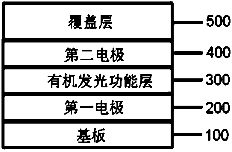
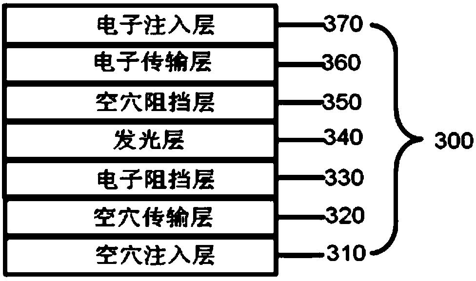
[0146] reference figure 1 The organic electroluminescence device of the present invention includes a substrate layer 100, a first electrode layer 200, an organic light-emitting function layer 300, a second electrode layer 400 and a cover layer 500.

[0147] A known method can be used to form a barrier layer (which can be composed of inorganic materials or / and organic materials to prevent foreign matter from penetrating the substrate and devices) and a wiring layer (which can include driving TFTs, capacitors, wires, and low-temperature polysilicon LTPS) on the substrate layer.

[0148] In a specific embodiment, the first electrode layer 200 may be a reflective...

Embodiment 1

[0160] An organic electroluminescence device is prepared by the following preparation steps, including:

[0161] On a low-temperature polysilicon (LTPS) substrate (substrate layer 100), a 7nm ITO film (first electrode layer 200) is formed by sputtering, and etched into the required pattern, and each is ultrasonically cleaned with deionized water, acetone, and ethanol. 15 minutes, and then treated in a plasma cleaner for 2 minutes; here, the ITO electrode layer is the anode, and the hole injection layer material HAT-CN is evaporated on the ITO anode layer by vacuum evaporation method, the thickness is 10nm, this layer As the hole injection layer 310; on the hole injection layer 310, the hole transport material NPB is evaporated by vacuum evaporation method, the thickness is 110nm, this layer is the hole transport layer 320, and can also be used as a microcavity adjustment layer; On the hole transport layer 320, the electron blocking material TCTA is evaporated by a vacuum evaporat...

Embodiment 2

[0163] The preparation method is the same as device embodiment 1, but the following device structure is adopted:

[0164] ITO(7nm) / HAT-CN(10nm) / NPB(150nm) / TCTA(10nm) / CBP:Ir(PPy) 3 (90:1 0 mass ratio, 90 mass% CBP)(40nm) / / TPBI(35nm) / LiF(1nm) / Yb(1nm) / Mg:Ag(1 0:90 mass ratio, 10 mass% Mg ) (14nm) / Compound 1 of the present invention (50nm).


PUM

PropertyMeasurementUnit
Thicknessaaaaaaaaaa

Abstract

The present invention relates to an organic light emission diode device coated with a capping layer and application thereof. The organic light emission diode device comprises: a substrate layer; a first electrode located on the substrate layer; an organic light emission functional layer located on the first electrode; a second electrode located on the organic light emission functional layer; and acapping layer located at one side, emitting the light, of the organic light emission diode device, wherein the capping layer comprises an organic compound, the organic compound of the capping layer comprises the following features that: the molecular weight is in a range of 500-1200, the organic compound comprises lone pair electrons, and the number of the lone pair electrons is not less than 2.The present invention further relates to the application of the organic light emission diode device coated with the capping layer for display or lighting devices.

Description

Technical field [0001] The present invention relates to an organic electroluminescence device, in particular to an organic electroluminescence device containing a capping layer and capable of effectively improving light extraction efficiency. Background technique [0002] Organic Light Emission Diodes (OLED: Organic Light Emission Diodes) device technology can be used to manufacture new display products as well as new lighting products. It is expected to replace existing liquid crystal displays and fluorescent lighting, and has a broad application prospect. The OLED device has a sandwich structure, including electrode layers and organic light-emitting functional layers sandwiched between different electrode layers. Various electrode layers, organic light-emitting functional layers and other related material layers are superimposed on each other according to the purpose. OLED device. The OLED device is a current-driven device. When a voltage is applied to the electrodes at both e...

Claims


Application Information

Patent Timeline
IPC IPC(8): H01L51/05H01L51/52
CPCH10K10/00H10K50/85H10K50/858H10K59/35C09K11/06H10K85/654H10K85/657H10K85/6572H10K85/6574
Inventor 张兆超李崇唐丹丹王立春
Owner JIANGSU SUNERA TECH CO LTD
Why Eureka
Try Eureka