
Semiconductor device manufacturing method, semiconductor device and electronic device

A manufacturing method and technology of electronic devices, which are applied in semiconductor/solid-state device manufacturing, semiconductor devices, semiconductor/solid-state device components, etc., can solve problems such as debris or micro-cracks, wafer fragmentation, device failure, etc., to reduce Chips or micro-cracks, reducing height differences, optimizing the effect of windows

Active Publication Date: 2019-07-09
SEMICON MFG INT (SHANGHAI) CORP +1
View PDF5 Cites 1 Cited by
  • Summary
  • Abstract
  • Description
  • Claims
  • Application Information

AI Technical Summary

Problems solved by technology

However, as the thickness of the device becomes thinner, it brings great challenges to the grinding process and the subsequent laser annealing (LTA) process
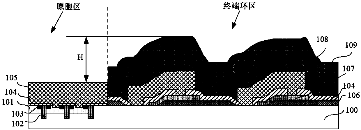
[0004] A typical IGBT structure includes a terminal ring area and a cell area (cell), wherein, on the front of the IGBT, due to the presence of a terminal ring structure in the terminal ring area and a protective layer covering the terminal ring area, such as a polyimide (polyimide) film layer, Causes a height difference between the terminal ring area and the cell area on the front side, which often leads to chips or microcracks in the back grinding thinning process
Debris leads to device failure, and microcracks also cause wafer fragmentation in the subsequent laser annealing process

Method used


Image

  • Semiconductor device manufacturing method, semiconductor device and electronic device
  • Semiconductor device manufacturing method, semiconductor device and electronic device
  • Semiconductor device manufacturing method, semiconductor device and electronic device

Examples


Embodiment Construction

[0040] In the following description, a lot of specific details are given in order to provide a more thorough understanding of the present invention. However, it is obvious to those skilled in the art that the present invention can be implemented without one or more of these details. In other examples, in order to avoid confusion with the present invention, some technical features known in the art are not described.

[0041] In order to thoroughly understand the present invention, a detailed description will be provided in the following description to illustrate the manufacturing method of the semiconductor device according to the present invention. Obviously, the implementation of the present invention is not limited to the specific details familiar to those skilled in the semiconductor field. The preferred embodiments of the present invention are described in detail as follows. However, in addition to these detailed descriptions, the present invention may also have other embodi...


PUM


Abstract

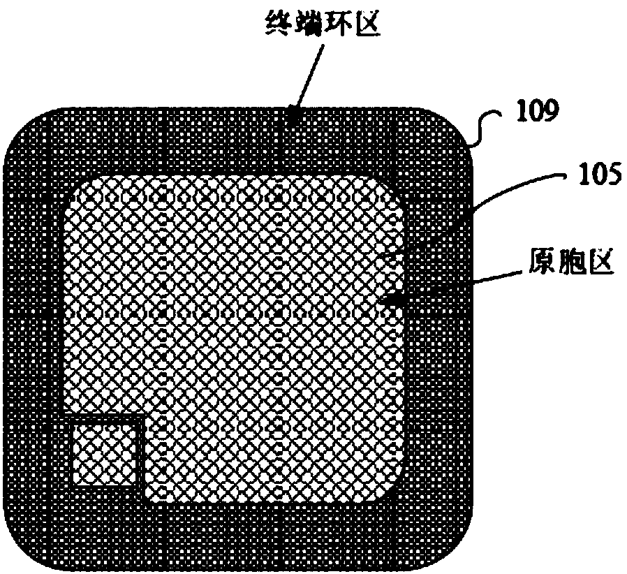
The invention provides a semiconductor device manufacturing method, a semiconductor device and an electronic device; the method comprises the following steps that a semiconductor substrate is provided, wherein a terminal ring region and a cell region are formed on the semiconductor substrate; and a protective layer for covering the terminal ring region and a supporting structure positioned on thecell region are formed on the semiconductor substrate, wherein the top of the supporting structure is lower than the top of the protective layer or is flush with the top of the protective layer. According to the manufacturing method of the semiconductor device, the semiconductor device and the electronic device, the supporting structure located in the cell region is formed on the semiconductor substrate, so that the height difference between the top of the cell region structure and the top of the structure of the terminal ring region is reduced before the back surface of a wafer is thinned, afilm stripping process and fragment risk due to the film stripping process caused by using an organic protective film as a buffer layer in the subsequent grinding thinning process can be avoided, theprocess flow is simplified, and meanwhile, the generation of fragments or micro-cracks is reduced.

Description

Technical field [0001] The present invention relates to the field of semiconductor manufacturing, in particular to a method of manufacturing a semiconductor device, a semiconductor device and an electronic device. Background technique [0002] Insulated gate bipolar transistor (IGBT) has become one of the most important high-power mainstream devices in the field of power electronics. As a high-power discrete device, reducing static (Vcesat) and dynamic (Eoff) power consumption has always been the development direction of IGBTs. In theory, static (Vcesat) and dynamic (Eoff) power consumption are mutually restricted (trade-off). [0003] The existing IGBT structure can realize the simultaneous optimization of static (Vcesat) and dynamic (Eoff) power consumption by further reducing the device thickness. This is also the development direction of a new generation of IGBTs of major international IGBT manufacturers. However, as the device thickness decreases, it brings great challenges...

Claims


Application Information

Patent Timeline
Patent Type & Authority Applications(China)
IPC IPC(8): H01L21/56H01L23/00
CPCH01L21/56H01L23/562
Inventor 高鹏
Owner SEMICON MFG INT (SHANGHAI) CORP
Learn More