A high-power ultraviolet light-emitting diode and its manufacturing method

A technology of light-emitting diodes and manufacturing methods, applied to semiconductor devices, electrical components, circuits, etc., can solve the problems of low quantum efficiency, weak current expansion effect, and multiple active area areas in deep ultraviolet light-emitting diodes, so as to ensure current expansion effect, improve the current expansion capability, and avoid the effect of area loss

Active Publication Date: 2020-05-01
XIAMEN CHANGELIGHT CO LTD
View PDF1 Cites 0 Cited by
  • Summary
  • Abstract
  • Description
  • Claims
  • Application Information

AI Technical Summary

Problems solved by technology

[0004] However, the increase in the number of n-type through holes will lose more active region area, resulting in low internal quantum efficiency of deep ultraviolet light-emitting diodes; the reduction in the number of through holes will lead to weaker current spreading effect
Therefore, the existing deep ultraviolet light-emitting diodes must make a trade-off between the area loss of the active region and the current spreading effect

Method used


Image

  • A high-power ultraviolet light-emitting diode and its manufacturing method
  • A high-power ultraviolet light-emitting diode and its manufacturing method
  • A high-power ultraviolet light-emitting diode and its manufacturing method

Examples


Embodiment 1

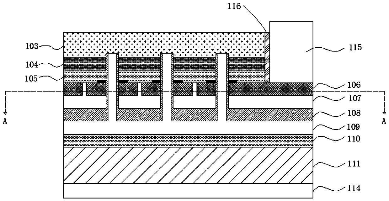
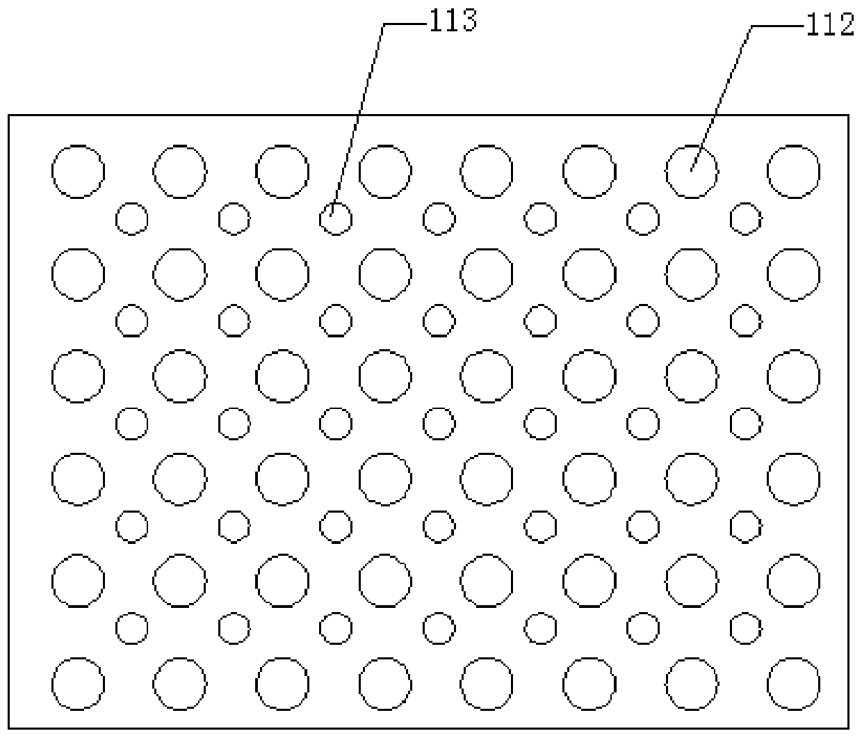
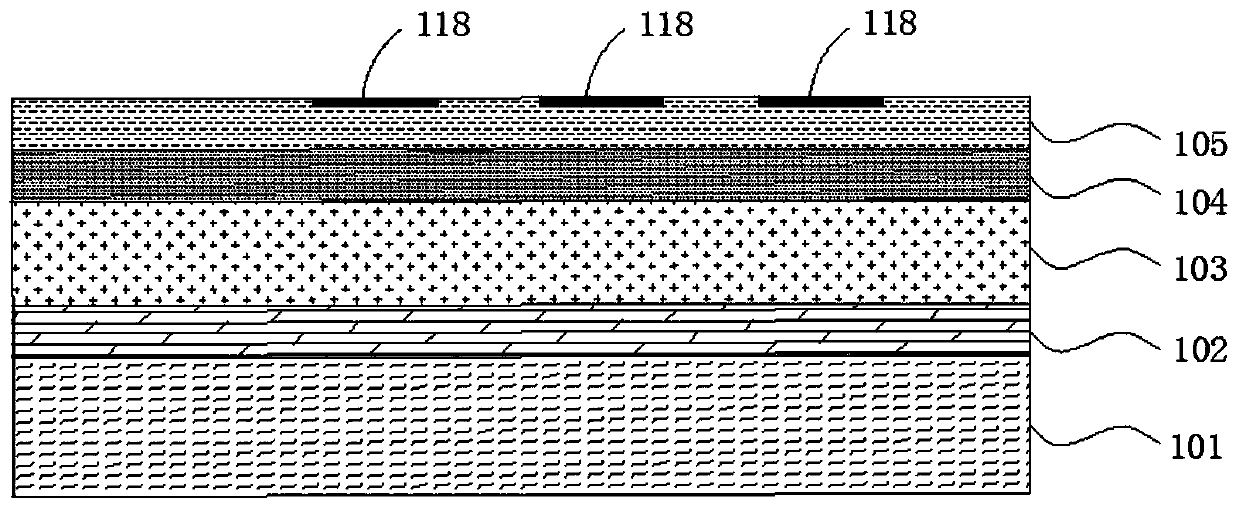
[0068] This embodiment provides a high-power ultraviolet light-emitting diode, such as figure 1 , 2 As shown, it includes: a conductive substrate 111, which has both front and back surfaces; a light-emitting structure, which is flip-chip welded on the front surface of the conductive substrate 111 through a metal bonding layer 110; A conductive semiconductor layer 103, an active layer 104, a second conductive semiconductor layer 105, a transparent conductive layer 106, a metal mirror 107, an isolation layer 108, and a conductive layer 109; a first conductive semiconductor layer 103, an active layer 104 1. The second conductive type semiconductor layer 105 constitutes the epitaxial layer of the ultraviolet light emitting diode; the transparent conductive layer 106 is provided with a number of uniformly distributed extended through holes 113, and each extended through hole 113 reveals part of the surface of the second conductive type semiconductor layer 105; Metal reflector 107 ...

Embodiment 2

[0091] This embodiment provides another high-power ultraviolet light-emitting diode, such as Figure 4 , 5 As shown, it includes: a conductive substrate 111, which has both front and back surfaces; a light-emitting structure, which is flip-chip welded on the front surface of the conductive substrate 111 through a metal bonding layer 110; A conductive semiconductor layer 103, an active layer 104, a second conductive semiconductor layer 105, a transparent conductive layer 106, a metal mirror 107, an isolation layer 108, and a conductive layer 109; a first conductive semiconductor layer 103, an active layer 104 1. The second conductive type semiconductor layer 105 constitutes the epitaxial layer of the ultraviolet light emitting diode; the transparent conductive layer 106 is provided with a number of uniformly distributed extended through holes 113, and each extended through hole 113 reveals part of the surface of the second conductive type semiconductor layer 105; Metal reflect...

Embodiment 3

[0115] This embodiment provides another high-power ultraviolet light-emitting diode, such as Figure 7 , 8 As shown, it includes: a conductive substrate 111, which has both front and back surfaces; a light-emitting structure, which is flip-chip welded on the front surface of the conductive substrate 111 through a metal bonding layer 110; A conductive semiconductor layer 103, an active layer 104, a second conductive semiconductor layer 105, a transparent conductive layer 106, a metal mirror 107, an isolation layer 108, and a conductive layer 109; a first conductive semiconductor layer 103, an active layer 104 1. The second conductive type semiconductor layer 105 constitutes the epitaxial layer of the ultraviolet light emitting diode; the transparent conductive layer 106 is provided with a number of uniformly distributed extended through holes 113, and each extended through hole 113 reveals part of the surface of the second conductive type semiconductor layer 105; Metal reflect...


PUM


Abstract

The invention provides a high-power ultraviolet light emitting diode and a manufacturing method thereof. Firstly, N-type through holes are arranged to electrically connect a conductive layer with a first conductive layer, which improves the current expansion capability of the ultraviolet light emitting diode. Secondly, uniformly-distributed expanded through-holes are formed in a transparent conductive layer to make the transparent conductive layer, a metal mirror and a second conductive layer form ohmic contact. The N-type through holes and the extended through holes are arranged in a staggered manner along the vertical direction of the transparent conductive layer. The number of the N-type through holes is reduced while the effect of current expansion is guaranteed, and the area loss of the active layer caused by too many through holes is avoided.

Description

technical field [0001] The invention belongs to the field of light-emitting diodes, in particular to a high-power ultraviolet light-emitting diode and a manufacturing method thereof. Background technique [0002] With the rapid development of light-emitting diode technology, deep ultraviolet light-emitting diodes have become a hot technology in light-emitting diodes. Deep ultraviolet light-emitting diodes have a wide range of applications, and have great application value in lighting, sterilization, medical treatment, printing, biochemical detection, high-density information storage, and secure communication. [0003] In order to solve the problem that the incorporation efficiency of P-type doping is low and the incorporation efficiency of N-type doping is not high because the deep-ultraviolet light-emitting diode is composed of AlGaN III-V compound with high Al composition, some deep-ultraviolet The LED device adopts a vertical structure and solves the above problems by pr...

Claims


Application Information

Patent Timeline
Patent Type & Authority Patents(China)
IPC IPC(8): H01L33/10H01L33/14H01L33/24H01L33/38H01L33/00
CPCH01L33/005H01L33/10H01L33/145H01L33/24H01L33/382H01L2933/0016
Inventor 林志伟陈凯轩卓祥景曲晓东蔡建九
Owner XIAMEN CHANGELIGHT CO LTD
Why Eureka
Try Eureka