Super-resolution defect detecting device and detecting method based on super-oscillation lens

A defect detection and super-oscillation technology, applied in the field of microscopic imaging and micro-nano optics, can solve problems such as insufficient resolution and achieve the effect of improving efficiency

Active Publication Date: 2019-07-19
INST OF OPTICS & ELECTRONICS - CHINESE ACAD OF SCI
View PDF3 Cites 8 Cited by
  • Summary
  • Abstract
  • Description
  • Claims
  • Application Information

AI Technical Summary

Problems solved by technology

[0006] The technical problem to be solved by the present invention is: to overcome the problem of insufficient resolution of the existing defect detection technology, a super-resolution imaging method based on a super-oscillating lens is proposed, and the design of super-resolution defect detection equipment is completed in combination with the autofocus system , improving the accuracy of substrate defect detection in the semiconductor processing industry

Method used


Image

  • Super-resolution defect detecting device and detecting method based on super-oscillation lens
  • Super-resolution defect detecting device and detecting method based on super-oscillation lens

Examples


Embodiment 1

[0039] Example 1: Using an auto-focus defect detection device based on image information entropy and hill-climbing search algorithm to measure a substrate with a minimum defect size of 100 nm or less

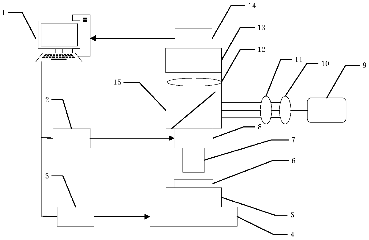
[0040] 1. Build the optical path: such as figure 1 As shown, the laser light source 9 emits laser light with a wavelength of 532nm, which is collimated by the beam expander 10 and the collimator lens 11 and irradiates the semi-transparent and semi-reflective lens 15, and the laser beam reaches the objective lens 7 with a magnification of 50 times after being reflected. Irradiated to the substrate 6 adsorbed in the vacuum adsorption device 5, the light beam reflected by the substrate passes through the semi-transparent and semi-reflective lens 15, then passes through the specially optimized super-oscillating lens 12, and finally reaches the CCD 14 through the microscope body 13 to complete the image collected, and then transmitted to the host computer 1. Among them, the speciall...

Embodiment 2

[0045] Example 2: Using an auto-focus defect detection device based on the improved point sharpness algorithm and hill-climbing search algorithm to measure a substrate with a minimum defect size of 100 nm or less

[0046] 1. If figure 1 As shown, the laser light source 9 emits the laser beam, reaches the semi-transparent lens 15 through the beam expander 10 and the collimator lens 11, and reaches the substrate 6 surface through the semi-transparent lens 15 and the objective lens 7, and the substrate 6 surface reflection The returned light passes through the semi-transparent and semi-reflective lens 15 again, and then transmits to the specially optimized super-oscillating lens 12 , and finally the digital image of the substrate 6 is collected by the CCD 14 in real time.

[0047] 2. Coarse focusing process: Still use the linear motor to drive the linear motor with the driver program in the upper computer 1, and use the image collected by the CCD to analyze, according to the form...


PUM


Abstract

The invention discloses a super-resolution defect detecting device and detecting method based on a super-oscillation lens. A workpiece table, a vacuum adsorption device, a substrate, a semi-transparent and semi-reflective mirror group, a laser light source, a collimating lens, an objective lens, a CCD, a piezoelectric motor, a linear motor, an upper computer and the like are used, so that a collimated laser light is irradiated to the semi-transparent and semi-reflective mirror group; the semi-transparent and semi-reflective mirror group reflects the laser light onto the substrate first; then the light reflected from the surface of the substrate passes through the semi-transparent and semi-reflective mirror, and then converges on the CCD through a specially optimized super-oscillation lens;and the process of automatic focusing is completed by using an image acquired by the CCD and a program in the host computer, and finally the defect detection of the substrate below 100 nm is realized. The super-resolution defect detecting device and detecting method based on the super-oscillation lens can be used for the detection of substrate defects in a lithography machine, and improves the yield of the lithography machine in actual industrial production.

Description

technical field [0001] The invention belongs to the field of microscopic imaging and micro-nano optics, and in particular relates to a super-resolution defect detection device and detection method based on a super-oscillation lens. Background technique [0002] In the process of modern semiconductor lithography, the surface quality of the substrate is one of the key factors determining the quality of the product. The main hazards of substrate defects are scattering, energy absorption, harmful flares, diffraction fringes, film damage, etc., which will affect the performance and normal operation of the system. If the surface quality problem of the substrate cannot be found in time and the process is adjusted in time, the loss will be very large, and the previous work on the substrate to be completed will be wasted. If the quality of the substrate surface can be detected in real time during the manufacturing process and fed back to the control system in time, and the entire pr...

Claims


Application Information

Patent Timeline
Patent Type & Authority Applications(China)
IPC IPC(8): G01N21/95G01N21/958G01N21/01
CPCG01N21/01G01N21/95G01N21/958G01N2021/0112G01N2021/9511G01N2021/9583
Inventor 罗先刚马晓亮李雄蒲明博鹿辛践
Owner INST OF OPTICS & ELECTRONICS - CHINESE ACAD OF SCI
Why Eureka
Try Eureka