Flexible conductive thin film, preparation method thereof and display panel
A flexible conductive and thin film technology, applied in the optical field, can solve the problems of limited flexibility, poor stability of the flexible conductive film, use reliability and life impact of the flexible conductive film, etc., so as to improve flexibility and use stability and improve service life. Effect
- Summary
- Abstract
- Description
- Claims
- Application Information
AI Technical Summary
Problems solved by technology
Method used
Image

Examples
preparation example Construction
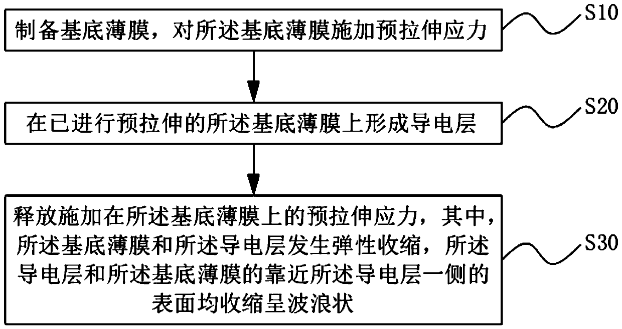
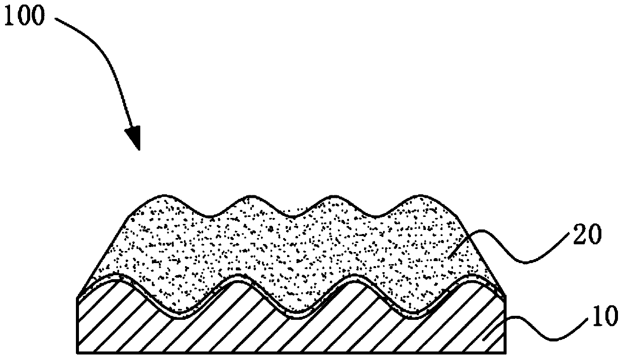
[0034] Such as figure 1 As shown, the preparation method of the flexible conductive film 100 includes: step S10, preparing the base film 10, applying pre-stretching stress to the base film 10; step S20, pre-stretching the base film 10 Forming a conductive layer 20; step S30, releasing the pre-stretching stress applied to the base film 10, wherein the base film 10 and the conductive layer 20 elastically shrink, and the conductive layer 20 and the base film 10, the surface of one side close to the conductive layer shrinks into a wave shape.
[0035] Such as Figure 6 As shown, the flexible conductive film 100 further includes a protective layer 30 disposed on the conductive layer 20 . The preparation method further includes: after the step S30 , forming the protective layer 30 on the conductive layer 20 .
[0036] The material of the protective layer is the same as that of the base film, and the material of the base film 10 is modified polydimethylsiloxane, such as bisamino-p...
Embodiment 1
[0043] Such as figure 2 As shown, the flexible conductive film 100 in this embodiment includes a base film 10 and a conductive layer disposed on the base film 10, wherein the conductive layer and the surface of the base film near the conductive layer are both It is wavy.
[0044] Such as figure 1 As shown, the preparation method of the flexible conductive film 100 includes:
[0045] Step S10, preparing the base film 10, and applying pre-tensioning stress to the base film 10;
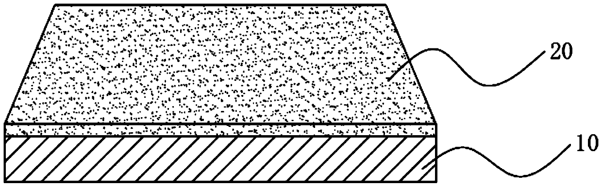
[0046] Such as image 3 and Figure 4 As shown, at first, prepare a bisamino-dimethylsiloxane film as the base film 10, and adjust the transparency of the base film 10 by pre-stretching stress, so that the transparency of the base film 10 reaches a set value, the The transparency of the base film 10 is controlled within a range of 55% to 88%. When the stretch rate of the base film 10 is 50%, the transparency of the base film 10 is 75%.
[0047] Step S20, forming a conductive layer 20 on the pre-st...
Embodiment 2
[0056] Such as Figure 6 As shown, the flexible conductive film further includes a protective layer 30 disposed on the conductive layer 20 , and the protective layer 30 covers the conductive layer 20 .
[0057] In this embodiment, on the basis of the preparation method in Embodiment 1, a flexible protective layer is added, so that the upper and lower surfaces of the conductive layer 20 form a flexible and transparent material with a protective effect.
[0058] After step S30 of Embodiment 1, prepare another layer of bisamino-polydimethylsiloxane film identical to the base film 10, and press the film on the conductive layer 20 by molding to form a protective layer 30 .
[0059] Likewise, when a crack occurs in the protective layer 30 , it can react with tritylaldehyde at room temperature to complete self-healing and crack repair.
[0060] The flexible conductive film in this embodiment has two layers of flexible transparent material protection, which can improve the stability...
PUM
| Property | Measurement | Unit |
|---|---|---|
| transparency | aaaaa | aaaaa |
Abstract
Description
Claims
Application Information
 - R&D
- Intellectual Property
- Life Sciences
- Materials
- Tech Scout
- Unparalleled Data Quality
- Higher Quality Content
- 60% Fewer Hallucinations
Browse by: Latest US Patents, China's latest patents, Technical Efficacy Thesaurus, Application Domain, Technology Topic, Popular Technical Reports.
© 2025 PatSnap. All rights reserved.Legal|Privacy policy|Modern Slavery Act Transparency Statement|Sitemap|About US| Contact US: help@patsnap.com