Flexible bioelectrode and preparation method thereof
A bioelectrode and flexible technology, applied in gaseous chemical plating, sensors, diagnosis, etc., can solve the problems of bioelectrode and skin contact impedance, achieve noise reduction, simple and efficient preparation method, and suitable for mass production
- Summary
- Abstract
- Description
- Claims
- Application Information
AI Technical Summary
Problems solved by technology
Method used
Image
Examples
no. 1 approach
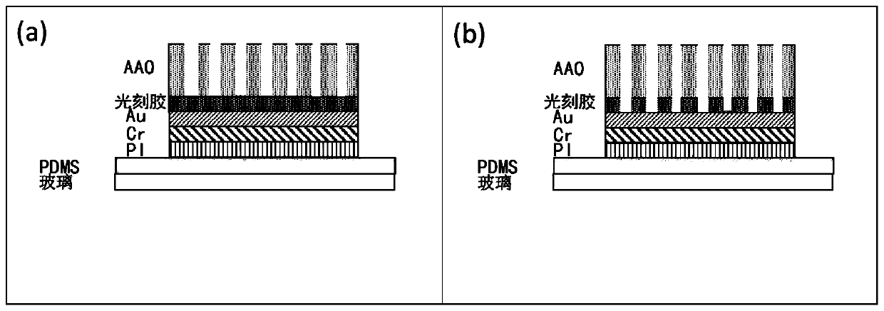
[0059] The first embodiment of the present invention provides a flexible bioelectrode, which includes: a conductive substrate 2; a one-dimensional conductive nanomaterial 1 formed on the On the surface of the conductive substrate 2, the diameter of the one-dimensional conductive nanomaterial 1 is 20 to 200 nm, and the length is 30 to 100 μm; wherein, at least in the contact interface area between the conductive substrate 2 and the one-dimensional conductive nanomaterial 1 has Polymer coating3.
[0060] The flexible bioelectrode of the present invention refers to a bioelectrode that still maintains normal functions during the process of bending, folding or even stretching deformation under the action of external force. In the present invention, by tightly fixing the one-dimensional conductive nanomaterial 1 on the conductive substrate 2, the one-dimensional conductive nanomaterial 1 can take advantage of its length-to-diameter ratio during the measurement of human body bioelect...
no. 2 approach
[0081] The second embodiment of the present invention provides a method for preparing the flexible bioelectrode according to the first embodiment of the present invention, which specifically includes the following steps:
[0082] A one-dimensional conductive nanomaterial is formed on the surface of the conductive substrate in such a manner that its axial direction is approximately perpendicular to the surface of the conductive substrate, the diameter of the one-dimensional conductive nanomaterial is 20-200 nm, and the length is 30-200 nm. 100μm;
[0083] A polymer solution is coated at least on the contact interface area between the conductive substrate and the one-dimensional conductive nanomaterial, and the polymer coating is formed after curing.
[0084] Typically, the present invention uses an anodized aluminum template with through holes, and uses electrochemical deposition or vapor deposition to grow one-dimensional conductive nanomaterials on the The surface of the con...
Embodiment
[0115] Embodiments of the present invention will be described in detail below in conjunction with examples, but those skilled in the art will understand that the following examples are only used to illustrate the present invention, and should not be considered as limiting the scope of the present invention. Those who do not indicate the specific conditions in the examples are carried out according to the conventional conditions or the conditions suggested by the manufacturer. The reagents or instruments used were not indicated by the manufacturer, and they were all commercially available conventional products.
[0116] Example
[0117] 1. Preparation of conductive substrate
[0118] In this embodiment, the conductive substrate is mainly composed of a flexible commercial polyimide (PI) film and an upper gold conductive layer. The commercial polyimide film has a thickness of 8 μm.
[0119] figure 2 Shown is the preparation process of the conductive substrate. Such as fig...
PUM
| Property | Measurement | Unit |
|---|---|---|
| Diameter | aaaaa | aaaaa |
| Length | aaaaa | aaaaa |
| Thickness | aaaaa | aaaaa |
Abstract
Description
Claims
Application Information


