Microarray integrated LED chip and preparation method thereof

An LED chip and microarray technology, applied in electrical components, electric solid state devices, circuits, etc., can solve the problems of high packaging technology requirements, high cost, complicated processes, etc., and achieve high luminous intensity, small size, and high brightness. Effect

Active Publication Date: 2019-08-02
XIANGNENG HUALEI OPTOELECTRONICS
View PDF7 Cites 7 Cited by
  • Summary
  • Abstract
  • Description
  • Claims
  • Application Information

AI Technical Summary

Problems solved by technology

This form, especially for some small-sized LED chips, is relatively complicated in the process of mass transfer, and requires high packaging technology. When connecting in series and parallel, there are many wires, the process is complicated and the cost is high.

Method used


Image

  • Microarray integrated LED chip and preparation method thereof
  • Microarray integrated LED chip and preparation method thereof
  • Microarray integrated LED chip and preparation method thereof

Examples


Embodiment Construction

[0037] The embodiments of the present invention will be described in detail below with reference to the accompanying drawings, but the present invention can be implemented in various ways defined and covered by the claims.

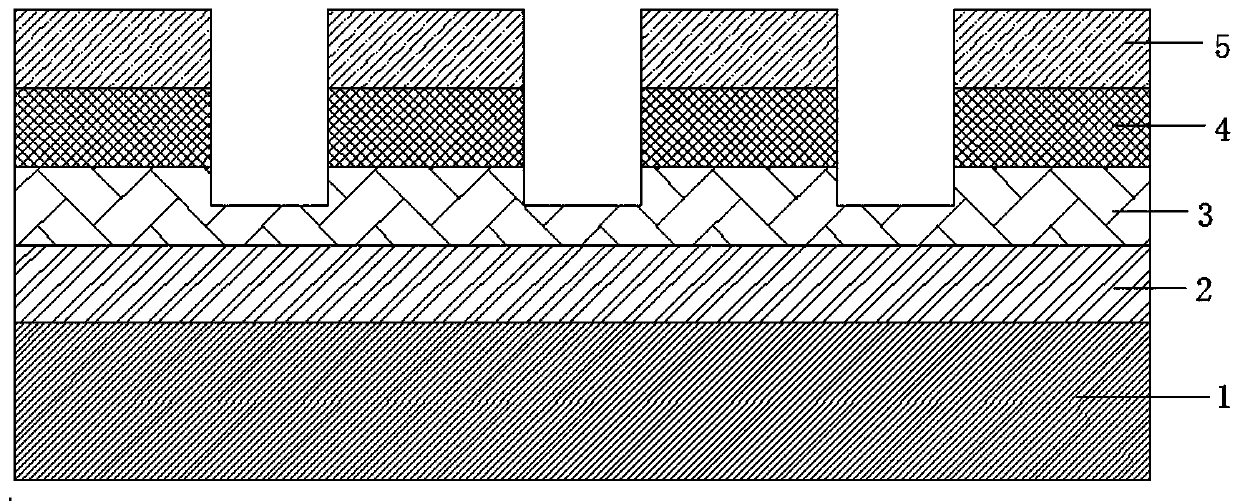
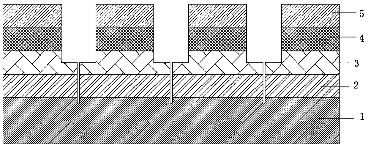
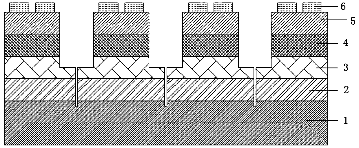
[0038] see Figure 1 to Figure 7 , a method for preparing a microarray integrated LED chip structure, comprising the following steps:

[0039] Step 1) Select an epitaxial wafer containing a GaN-based LED epitaxial structure, and its epitaxial wafer structure includes a substrate, a buffer layer, an N-type semiconductor layer (N-type GaN layer), a multi-quantum well layer (MQW) and a P type semiconductor layer (P-type GaN layer).

[0040]Step 2) First use the yellow light lithography process and the inductively coupled plasma (ICP) etching process to etch the N-type GaN layer from the P-type GaN layer around the epitaxial wafer in an array manner, exposing the N-type GaN layer mesa, The depth of etching from the P-type GaN layer to the N-type GaN layer by...


PUM


Abstract

The invention provides a microarray integrated LED chip comprising multiple GaN-based LED chips connected through an array structure. The adjacent GaN-based LED chips are connected through a transparent insulating layer and the substrate has an integrated structure. Each GaN-based LED chip structure comprises the substrate, a buffer layer, an N-type GaN layer, an MQW layer, a P-type GaN layer, anITO layer and the transparent insulating layer which are arranged from bottom to top in turn. Each GaN-based LED chip also comprises a first mesa penetrating to the N-type GaN layer from top to bottomand a second mesa penetrating from the N-type GaN layer to the substrate. An N electrode is arranged on the first mesa of the N-type GaN layer and the end part is exposed outside the transparent insulating layer. A P electrode penetrates through the transparent insulating layer and the ITO layer to be connected with the P-type GaN layer. The invention also provides a preparation method of the microarray integrated LED chip. The microarray integrated LED chip has the advantages of high density integrated packaging and high brightness and can also realize rapid overall transfer and packaging ofsmall-size chips.

Description

technical field [0001] The invention relates to the technical field of semiconductor LEDs, in particular to a microarray integrated LED chip and a preparation method thereof. Background technique [0002] At present, LED (Light Emitting Diode, light-emitting diode) is a light-emitting device made of GAN materials. Its advantages such as small size, low power consumption, long service life, high brightness, environmental protection, and durability are recognized by consumers. , The scale of domestic production of LED is also gradually expanding. At present, LED chips are mainly used in various aspects of production and life such as daily lighting, display, signal lights, car lights, agriculture, and medical care. [0003] At present, the main structures of LED chip preparation are three categories: front-mount structure, flip-chip structure, and vertical structure. However, most of these LED lamp beads use a plurality of chips to be packaged in a bracket with a circuit stru...

Claims


Application Information

Patent Timeline
Patent Type & Authority Applications(China)
IPC IPC(8): H01L27/15H01L33/36H01L33/62
CPCH01L27/156H01L33/36H01L33/62H01L2933/0016H01L2933/0066
Inventor 周智斌
Owner XIANGNENG HUALEI OPTOELECTRONICS
Why Eureka
Try Eureka