
Polycrystalline silicon ingot mould, application method and coating preparation method

A technology for polycrystalline silicon ingots and silicon ingots, which is applied to the growth of polycrystalline materials, chemical instruments and methods, crystal growth, etc., can solve the problems of no coating, and the silicon ingots are not easy to take out, so as to reduce the difficulty of drafting and improve the drafting efficiency. Effect

Active Publication Date: 2019-08-06
新疆泰宇达环保科技有限公司
View PDF5 Cites 2 Cited by
  • Summary
  • Abstract
  • Description
  • Claims
  • Application Information

AI Technical Summary

Problems solved by technology

[0003] The purpose of the present invention is to provide a polysilicon ingot mold and its use method, coating preparation method, to solve the problems in the prior art that the silicon ingot is not easy to take out from the mold after molding, and there is no coating that can match the polysilicon mold in the prior art. To solve the problem, to achieve the purpose of easy drawing, without polluting the molded silicon products, and to ensure that the polysilicon mold can give full play to its own advantages in the process of industrial silicon molding

Method used


Image

  • Polycrystalline silicon ingot mould, application method and coating preparation method
  • Polycrystalline silicon ingot mould, application method and coating preparation method
  • Polycrystalline silicon ingot mould, application method and coating preparation method

Examples


Embodiment 1

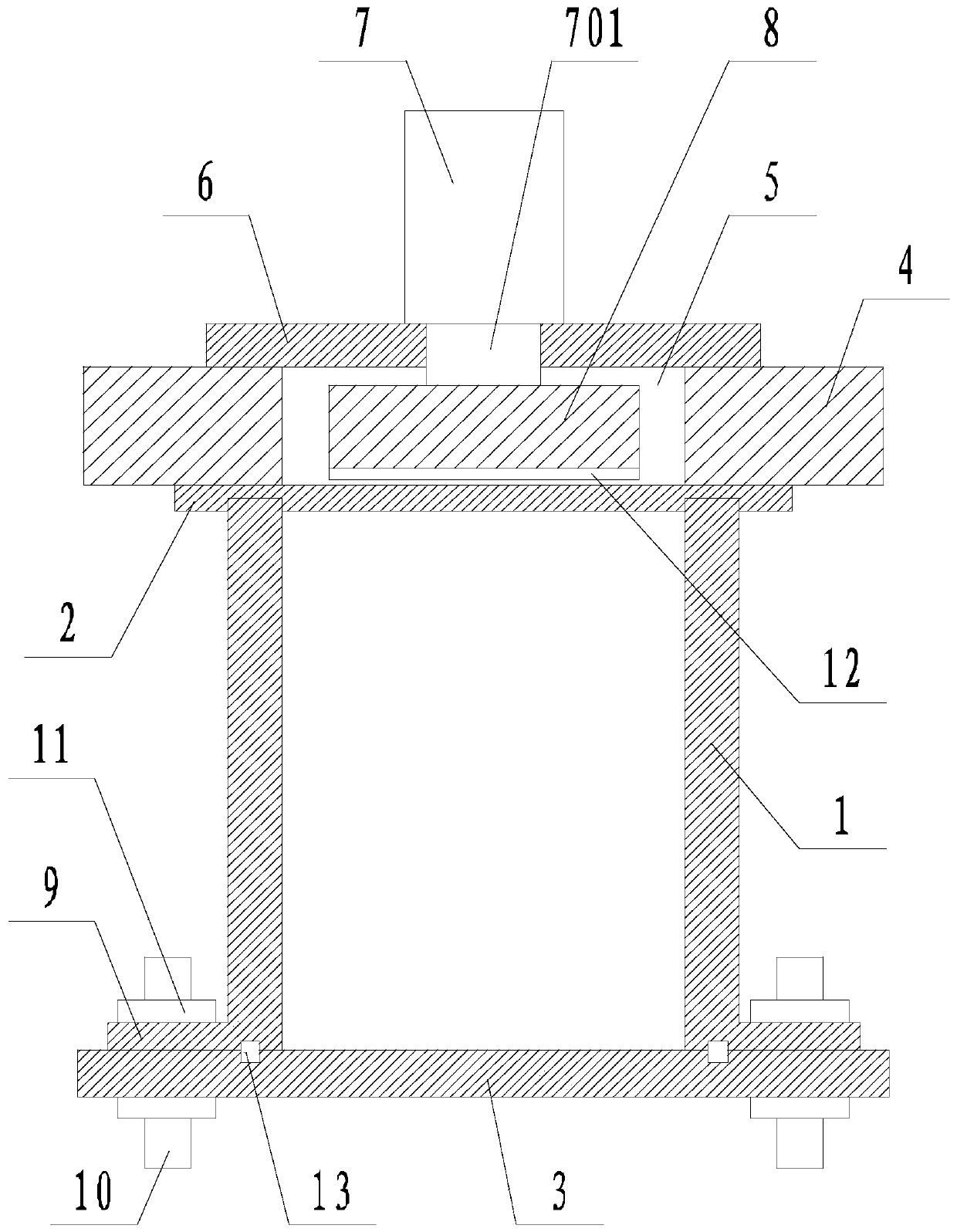
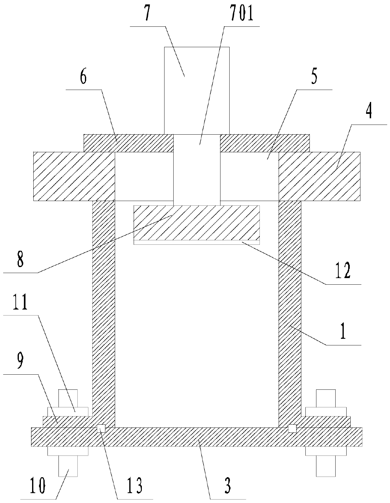
[0044] Such as figure 1 and figure 2 A polysilicon ingot mold shown includes a mould. The mold includes a side wall 1, a mold top 2, and a mold bottom 3. The upper and lower ends of the side wall 1 are open, and the mold top 2 is placed on the side wall. 1, the bottom of the mold 3 is detachably connected to the bottom of the side wall 1, and the holding part 4 is placed on the top of the mold 2, and the through hole 5 communicating up and down is opened on the holding part 4. The mounting plate 6 is fixed, and the linear driving device 7 with the driving end 701 facing downward is arranged on the mounting plate 6. The driving end 701 of the linear driving device 7 passes through the mounting plate 6 and enters the through hole 5. The driving end The bottom of 701 is fixedly connected to the draft push plate 8; the side wall 1, the mold top 2, and the mold bottom 3 are all made of polysilicon material; the inner surface of the side wall 1, the bottom surface of the mold top ...

Embodiment 2

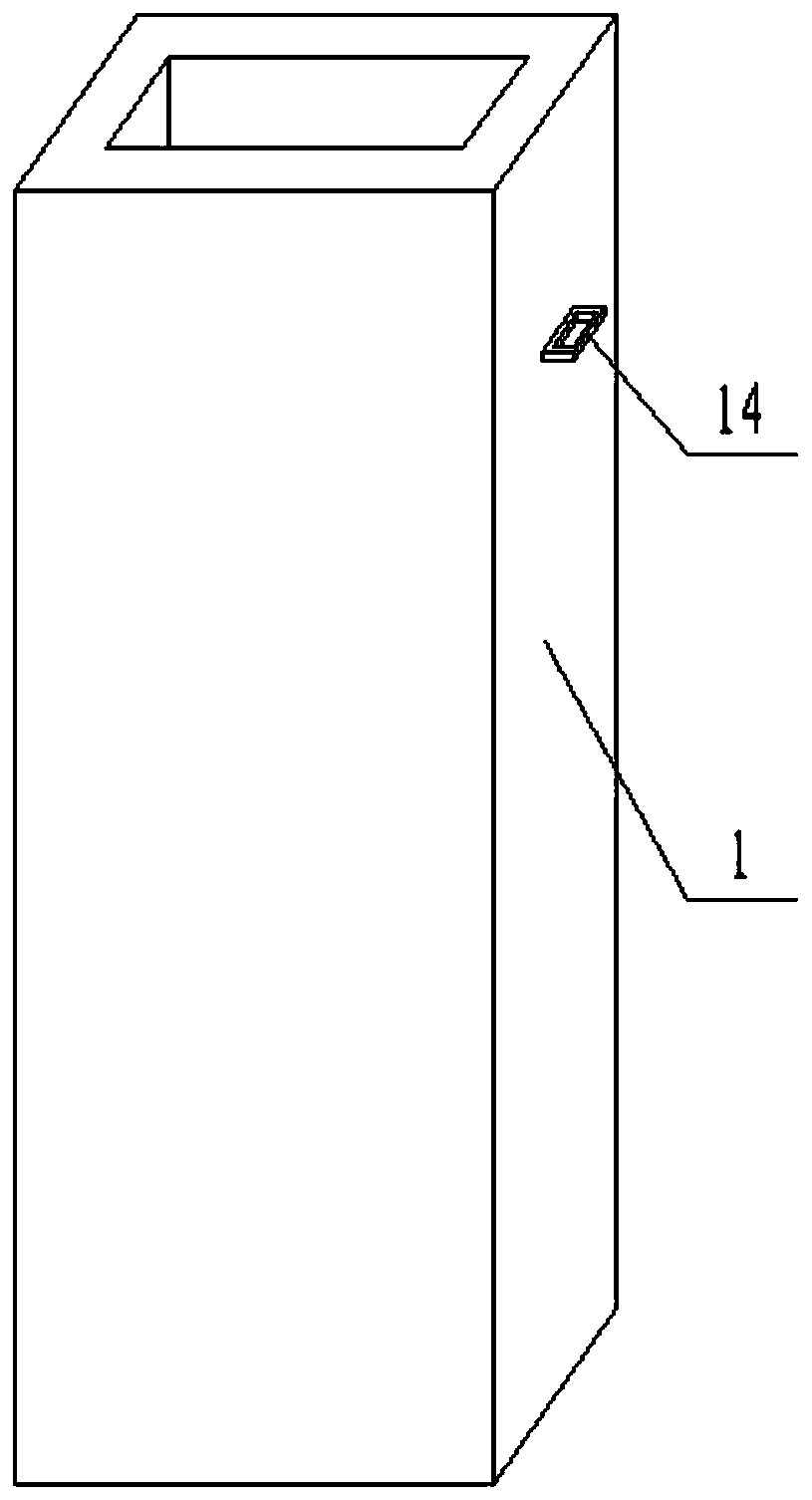
[0046] Such as figure 1 and figure 2In the shown polysilicon ingot mold, on the basis of Example 1, the side wall 1 is a cuboid structure with open upper and lower ends and a hollow interior; the opposite sides of the side wall 1 are fixed with lifting lugs 14 . The bottom surface of the mold top 2 is provided with a slot matching the top of the side wall 1, and the top of the side wall 1 is inserted into the slot; flange 9, the bottom surface of the flange 9 is in contact with the upper surface of the mold bottom 3, and also includes bolts 10 penetrating through the flange 9 and the mold bottom 3, and nuts 11 are sleeved at the upper and lower ends of the bolt 10; 4 is a stainless steel plate; the mounting plate 6 is welded to the holding member 4 . A layer of rubber pad 12 is laid on the bottom surface of the draft push plate 8; the thickness of the rubber pad 12 is 1-2 cm. The use process of this embodiment is as follows:

[0047] (A) The mold bottom 3 is placed flat ...

Embodiment 3

[0055] The preparation method of big ingot paint, comprises the following steps:

[0056] (a) Fully grind and mix 50 parts of silicon carbide, 25-30 parts of silicon nitride, 10-12 parts of calcium silicate, 15-20 parts of bentonite, 6-8 parts of adhesive, and 1-2 parts of graphite powder;

[0057] (b) Put the mixed raw materials into a reaction kettle, add a solvent, and stir for 30 minutes at 85-90°C under normal pressure;

[0058] (c) Add 8 to 10 parts of sodium tripolyphosphate, 3 to 5 parts of acrylamide and / or polyacrylamine into the reaction kettle, raise the temperature in the kettle to 150~200°C, and raise the pressure in the kettle to 1.5~ 2 times atmospheric pressure, stirring for 60min;

[0059] (d) discharge to normal pressure in the reaction kettle, make the inside of the reaction kettle be cooled to room temperature;

[0060] (e) The finished product in the reactor should be sealed and stored.

[0061] Preferably, in the process of cooling the interior of the...


PUM

PropertyMeasurementUnit
Thicknessaaaaaaaaaa

Abstract

The invention discloses a polycrystalline silicon ingot mould, an application method and a coating preparation method. The side wall, the top and the bottom of the mould are all made of a polycrystalline silicon material, so the polycrystalline silicon ingot mould is fast to cool, does not pollute silicon products and does not interfere with the purity of silicon ingots. A large ingot coating is specially used in an industrial silicon forming mold made of polycrystalline silicon as a raw material, the problem that no coating is matched with a polycrystalline silicon mold in the prior art can be solved, and the large ingot coating can ensure that the polycrystalline silicon mold maintains the advantages of fast heat transfer and no pollution, thereby improving the forming quality of the silicon ingots. The large ingot coating abandons the mode that a traditional mold coating uses carbon or carbon-containing organic matters as a coating main agent, and uses a silicon-based main agent tocooperate with the polycrystalline silicon mold used for industrial silicon production. Silicon carbide and silicon nitride can ensure that impurity pollution is not caused to silicon material molding, and also have excellent adaptability with polycrystalline silicon, so that the coating does not pollute industrial silicon while ensuring that the polycrystalline silicon does not pollute the industrial silicon.

Description

technical field [0001] The invention relates to the field of industrial silicon, in particular to a polycrystalline silicon ingot mold, a method for using it, and a method for preparing a paint. Background technique [0002] Industrial silicon, also known as metal silicon, is mainly used as an additive for non-ferrous alloys. Metal silicon is a product smelted from quartz and coke in an electric furnace. The main component silicon content is about 98% (in recent years, 99.99% of Si content is also included in metal silicon), and the remaining impurities are iron and aluminum. , calcium, etc. Silicon is widely used in smelting into ferrosilicon alloy as an alloying element in the iron and steel industry, and as a reducing agent in the smelting of many kinds of metals. Silicon is also a good component in aluminum alloys, and most cast aluminum alloys contain silicon. Silicon is the raw material of ultra-pure silicon in the electronics industry. Electronic devices made of ul...

Claims


Application Information

Patent Timeline
IPC IPC(8): C30B28/06C30B29/06C04B35/66
CPCC04B35/66C30B28/06C30B29/06
Inventor 庹开正周旭
Owner 新疆泰宇达环保科技有限公司
Learn More