Substrate adsorption device, photoetching equipment and adsorption method

A technology of adsorption device and substrate, which is applied in the direction of microlithography exposure equipment, photomechanical equipment, exposure device of photo-plate making process, etc., can solve the problem of lower reliability of silicon wafer, lower reliability of adsorption, affecting the exposure quality of silicon wafer and good quality of silicon wafer. Ratio and other issues, to achieve the effect of improving exposure quality and yield, and improving production efficiency

Inactive Publication Date: 2019-08-13
SHANGHAI MICRO ELECTRONICS EQUIP (GRP) CO LTD
View PDF5 Cites 5 Cited by
  • Summary
  • Abstract
  • Description
  • Claims
  • Application Information

AI Technical Summary

Problems solved by technology

With the development of Through Silicon Vias (TSV) technology, the continuous thinning of silicon wafers and the bonding process of silicon wafers lead to uncertain warping of the silicon wafer itself. A gap is formed on the surface. When the suction cup turns on the vacuum, there will be a vacuum leak between the suction cup and the silicon wafer, which cannot meet the vacuum threshold under normal conditions, resulting in a decrease in the reliability of the silicon wafer adsorption, and even the occurrence of the chip, which greatly affects productivity
In addition, the reduced reliability of silicon wafer adsorption will affect the focal depth (focus) and overlay accuracy (overlay) of lithography equipment, which is reflected in the surface accuracy of its upper and lower surfaces and its own clamping deformation, thus affecting the exposure quality of silicon wafers and wafer yield
[0004] The existing lithography equipment has improved the suction cup. Although it can absorb silicon wafers with a warpage of 1mm, it still cannot absorb silicon wafers with a large warpage.

Method used


Image

  • Substrate adsorption device, photoetching equipment and adsorption method
  • Substrate adsorption device, photoetching equipment and adsorption method
  • Substrate adsorption device, photoetching equipment and adsorption method

Examples


Embodiment 1

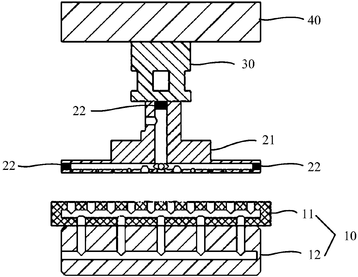
[0043] This embodiment provides a substrate adsorption device, figure 1 For the sectional view of the substrate adsorption device provided in Embodiment 1 of the present invention, refer to figure 1 , the substrate adsorption device includes an adsorption mechanism 10, and a shaping mechanism arranged opposite to the adsorption mechanism 10, and a substrate accommodation space is formed between the adsorption mechanism 10 and the shaping mechanism;

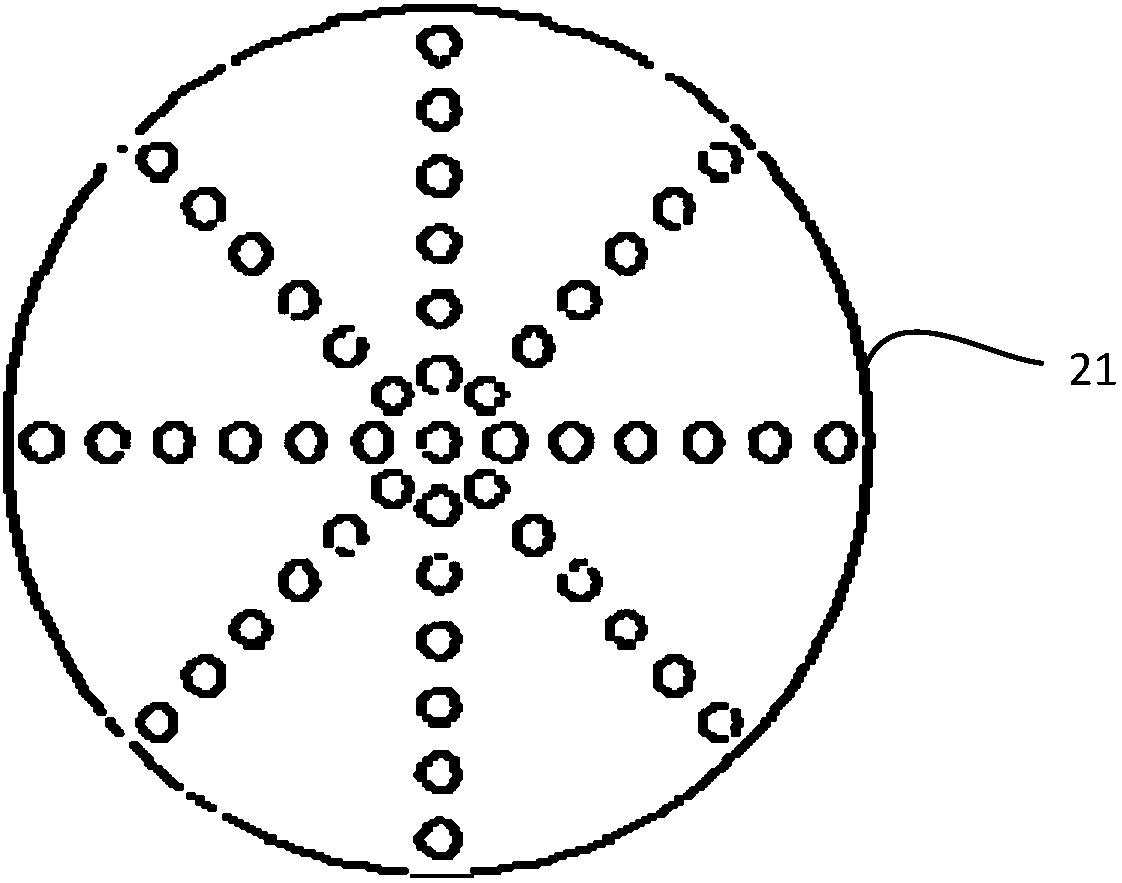
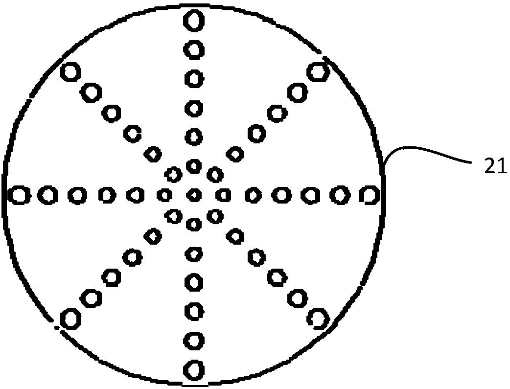
[0044] The adsorption mechanism 10 includes a suction cup 11, a plurality of suction holes are distributed on the surface of the suction cup 11, and the suction cup 11 is used to adsorb the substrate in the substrate accommodation space from the first side;

[0045] The shaping mechanism is used to act on the substrate in the substrate accommodating space from the second side opposite to the first side, so as to cooperate with the suction cup 11 to level the substrate in the substrate accommodating space.

[0046] Exemplarily, in...

Embodiment 2

[0063] This embodiment provides a lithographic equipment, the lithographic equipment includes the substrate adsorption device in the first embodiment, refer to figure 1 , the substrate adsorption device includes an adsorption mechanism 10, and a shaping mechanism arranged opposite to the adsorption mechanism 10, and a substrate accommodation space is formed between the adsorption mechanism 10 and the shaping mechanism;

[0064] The adsorption mechanism 10 includes a suction cup 11, a plurality of suction holes are distributed on the surface of the suction cup 11, and the suction cup 11 is used to adsorb the substrate in the substrate accommodation space from the first side;

[0065] The shaping mechanism is used to act on the substrate in the substrate accommodating space from the second side opposite to the first side, so as to cooperate with the suction cup 11 to level the substrate in the substrate accommodating space.

[0066] The lithography equipment provided by the embo...

Embodiment 3

[0068] This embodiment provides an adsorption method for a substrate adsorption device, wherein, refer to figure 1 , the substrate adsorption device includes an adsorption mechanism 10, and a shaping mechanism opposite to the adsorption mechanism, Figure 7 is the flowchart of the adsorption method, such as Figure 7 As shown, the adsorption method includes:

[0069] S11: the adsorption mechanism absorbs the substrate sheet from the first side of the substrate through the suction hole on the suction cup.

[0070] Specifically, after the substrate is transferred to the adsorption mechanism 10, the adsorption mechanism starts to evacuate, and through the suction holes on the surface of the suction cup 11, a vacuum is formed between the first side of the silicon wafer and the suction cup 11, thereby initially adsorbing the substrate on the suction cup. 11 on. Exemplarily, in this embodiment, the finite element simulation conditions are selected as follows: the substrate is a s...


PUM


Abstract

The invention discloses a substrate adsorption device, photoetching equipment and an adsorption method, the adsorption device comprises an adsorption mechanism and a shaping mechanism arranged opposite to the adsorption mechanism, and a substrate accommodating space is formed between the adsorption mechanism and the shaping mechanism; the adsorption mechanism comprises a sucker, a plurality of suction holes are distributed in the surface of the sucker, and the sucker is used for adsorbing the substrate in the substrate accommodating space from the first side; the shaping mechanism is used foracting on the substrate in the substrate containing space from the second side opposite to the first side so as to be matched with the suction cup to level the substrate in the substrate containing space. According to the embodiment of the invention, the shaping mechanism opposite to the adsorption mechanism is arranged; the adsorption mechanism flattens the substrate through cooperation of the suction holes in the sucker, the adsorption substrate sheet, the shaping mechanism and the sucker, so that the substrate is completely adsorbed on the sucker, flattening and complete adsorption of the substrate with the large warping amount are achieved, the exposure quality and yield of the substrate are improved, and the production efficiency is improved.

Description

technical field [0001] Embodiments of the present invention relate to the field of semiconductor manufacturing, and in particular, to a substrate adsorption device, photolithography equipment and an adsorption method. Background technique [0002] In the semiconductor process, the pattern of the mask plate is imaged on the substrate coated with photoresist by photolithography equipment. The substrate may be a silicon wafer, and the silicon wafer is usually fixed by a suction cup on the wafer stage. The wafer carrier drives the suction cup with the silicon wafer to move, and reaches the correct position according to the predetermined route and speed, and completes the photolithography process. [0003] Since the surface of the silicon wafer needs to be coated with photoresist, the silicon wafer is often fixed by adsorption. Among them, vacuum adsorption uses vacuum for contact adsorption, which is easy to implement and low in cost, and is currently a commonly used silicon wa...

Claims


Application Information

Patent Timeline
Patent Type & Authority Applications(China)
IPC IPC(8): G03F7/20H01L21/683
CPCG03F7/707H01L21/6838
Inventor 蔡晨齐芊枫王鑫鑫
Owner SHANGHAI MICRO ELECTRONICS EQUIP (GRP) CO LTD
Why Eureka
Try Eureka