A high-speed igbt device with ultra-low conduction voltage drop

A technology for conducting voltage drop and device, applied in the direction of semiconductor devices, electrical components, circuits, etc., can solve the problems of small short-circuit safe working area, large gate drive loss, low turn-off speed, etc., to improve the short-circuit safe working area, Avoid device failure or failure, prevent the effect of high potential

Active Publication Date: 2020-12-29
UNIV OF ELECTRONICS SCI & TECH OF CHINA
View PDF11 Cites 0 Cited by
  • Summary
  • Abstract
  • Description
  • Claims
  • Application Information

AI Technical Summary

Problems solved by technology

[0004] The purpose of the present invention is to propose a new type of slot-gate IGBT with a carrier storage layer for the problems of high turn-on voltage drop, low turn-off speed, small short-circuit safe working area and large gate drive loss. Groove gate IGBT in the carrier storage layer; the new groove gate IGBT is fully compatible with the existing groove gate IGBT process without any redundant process steps and costs

Method used


Image

  • A high-speed igbt device with ultra-low conduction voltage drop
  • A high-speed igbt device with ultra-low conduction voltage drop
  • A high-speed igbt device with ultra-low conduction voltage drop

Examples


Embodiment 1

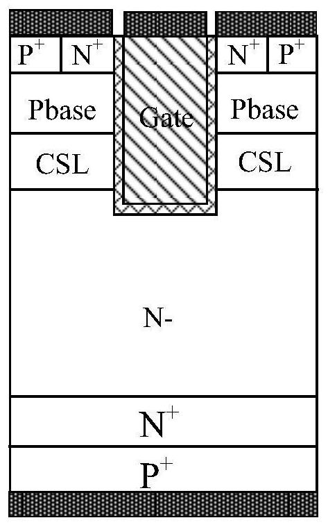
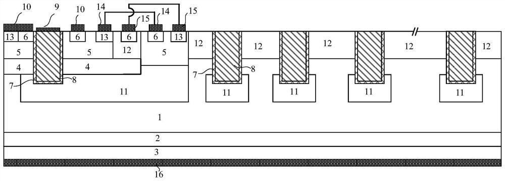
[0027] This embodiment provides a high-speed IGBT device with an ultra-low conduction voltage drop, and its cell structure and junction terminals are as follows image 3 As shown, it includes: a lightly doped N-type withstand voltage region 1, an N-type semiconductor region 2 arranged on the lower surface of the N-type withstand voltage region, forming an electric field termination layer, and a P-type collector region 3 arranged on the lower surface of the N-type semiconductor region 2 , the collector metal 16 covered on the lower surface of the P-type collector region 3, and the cell region and junction terminal region set on the upper surface of the N-type withstand voltage region 1;

[0028] The cell region includes: an epitaxial layer 12 disposed on the upper surface of the N-type withstand voltage region 1, a first P-type base region, a second P-type base region and a third IGBT base region disposed in the epitaxial layer 12. P-type base region, the first N-type carrier s...

Embodiment 2

[0031] This embodiment provides a high-speed IGBT device with an ultra-low conduction voltage drop, and its cell structure and junction terminals are as follows Figure 4 As shown, the difference between it and Embodiment 1 is that the deep groove is composed of a filling medium 17 filled in the groove.

Embodiment 3

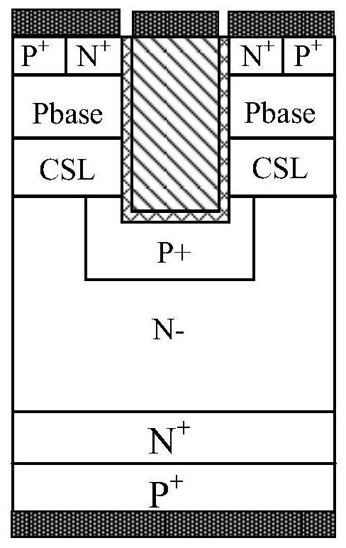
[0033] This embodiment provides a high-speed IGBT device with an ultra-low conduction voltage drop, and its cell structure and junction terminals are as follows Figure 5 As shown, the difference from Example 1 is that in the cellular region, an isolation region is also provided between the epitaxial layer and the third P-type base region, and the isolation region adopts the same structure as the trench gate , is also composed of a silicon dioxide gate dielectric layer 7 on the groove wall and a polysilicon gate 8 in the groove, and the polysilicon gate 8 is connected to the first connection metal 14, or is connected to the second connection metal 15, or is not connected to any region connected.


PUM


Abstract

The invention relates to the field of power semiconductors, and provides a high-speed IGBT device with an ultra-low conduction voltage drop, which is used to overcome the high conduction voltage drop, low turn-off speed, and short-circuit safety of the existing slot-gate IGBT with a carrier storage layer. The problem of small working area and large gate drive loss. The IGBT device of the present invention integrates two diodes connected in series on the surface of the silicon wafer to clamp the potential of the P-type electric field shielding layer by using the same process doping, so that the doping concentration of the CSL layer can be increased by 3-4 orders of magnitude; the weight of the CSL layer Doping greatly improves the electron injection efficiency of the IGBT emitter, thereby greatly improving the trade-off relationship between the turn-on voltage drop and turn-off loss of the IGBT at a lower channel density; at the same time, due to the clamping of the diode Bit action, so that the drain near the nMOS channel of the IGBT is clamped at a lower voltage under high voltage and high current, so that the saturation current density of the new IGBT is greatly reduced, thereby improving the short-circuit safe operating area of ​​the IGBT .

Description

technical field [0001] The invention relates to the field of power semiconductors, and provides a slot gate IGBT device using a surface diode to clamp the potential of the carrier layer and a carrier storage layer, specifically a device with ultra-low conduction voltage drop, low saturation current density and fast turn-off characteristics of IGBT devices. Background technique [0002] IGBT compromises the low turn-on voltage drop of BJT and the fast switching characteristics of MOSFET, so it is widely used in power electronic systems. The difficulty in designing an IGBT lies in the compromise between low turn-on voltage drop, low turn-off loss, high safe operating area, and low gate drive loss. When the IGBT is turned on, the collector injects a large number of unbalanced carriers into the withstand voltage region to reduce the conduction voltage drop. When it is turned off, the minority carriers in the withstand voltage region will take a while to disappear, thus making t...

Claims


Application Information

Patent Timeline
Patent Type & Authority Patents(China)
IPC IPC(8): H01L29/739H01L29/06
CPCH01L29/0634H01L29/0696H01L29/7397
Inventor 易波蔺佳陈星弼
Owner UNIV OF ELECTRONICS SCI & TECH OF CHINA
Why Eureka
Try Eureka