Graphene photoelectric detector with sub-wavelength metal grating structure

A photodetector and metal grating technology, applied in the field of optical communication, can solve the problems of low detector responsivity and low light absorption efficiency of graphene, and achieve the effect of improving responsivity and enhancing light absorption

Active Publication Date: 2019-08-16
HUNAN INST OF TECH
View PDF4 Cites 4 Cited by
  • Summary
  • Abstract
  • Description
  • Claims
  • Application Information

AI Technical Summary

Problems solved by technology

Graphene photodetectors have extremely high carrier mobility and have great potential for development in the field of high-speed optical communications. The structure of the absorption layer of traditional graphene photodetectors is to set a layer of graphene that absorbs light on the surface of the substrate. , but due to the low light absorption efficiency of graphene, the responsivity of the detector is low

Method used


Image

  • Graphene photoelectric detector with sub-wavelength metal grating structure
  • Graphene photoelectric detector with sub-wavelength metal grating structure
  • Graphene photoelectric detector with sub-wavelength metal grating structure

Examples


Embodiment 1

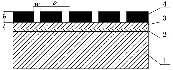
[0029] The graphene photodetector structure of the present embodiment sees figure 1 As shown, wherein the grating period is 400nm, the slit width is 100nm, the grating height is 240nm, the thickness of the buffer layer 3 is 20nm, and the buffer layer 3 is made of silicon material. The sub-wavelength metal grating is made of silver material, and its relative permittivity is the Drude model:

[0030]

[0031] In formula (1), γ and ω represent the electron collision frequency and the angular frequency of the incident light respectively, i is the imaginary unit, ε ∞ and ω p are the infinite frequency dielectric constant and the surface plasmon frequency, respectively.

[0032] The relative permittivity of graphene 2 is ε g =1+iσ g / ωε 0 Δ, Δ is the thickness of single-layer graphene 2, ω is the angular frequency of the incident light, i is the imaginary unit, ε 0 is the vacuum permittivity, σ g is the conductivity constant, σ g = σ intra +σ inter ,in

[0033]

[0...

Embodiment 2

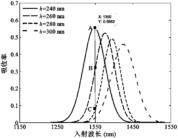
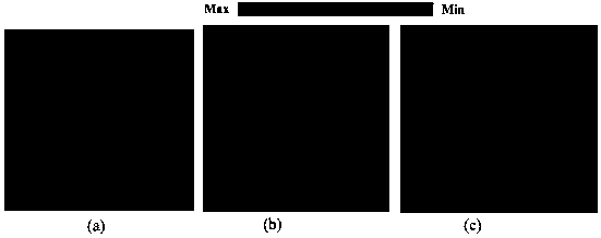
[0038] The structure of the graphene photodetector in this embodiment is the same as that in Embodiment 1, except that the grating height is 260 nm. figure 2 Also shows the light absorption spectrum figure of the graphene photodetector involved in the present embodiment, in addition image 3 It also shows the corresponding COMSOL software simulation electric field distribution diagram (see image 3 in part b).

Embodiment 3

[0040] Same as the structure of embodiments 1 and 2, the difference is that the height of the grating in this embodiment is 280nm, figure 2 The light absorption spectrum of the graphene photodetector involved in this embodiment is shown in image 3 The corresponding COMSOL software simulation electric field distribution diagram is shown in (see image 3 in part c).


PUM

PropertyMeasurementUnit
Heightaaaaaaaaaa
Slit widthaaaaaaaaaa
Thicknessaaaaaaaaaa

Abstract

A graphene photoelectric detector with a sub-wavelength metal grating structure relates to the technical field of optical communication. The photoelectric detector includes a substrate and an absorption layer. The absorption layer includes a single layer of graphene attached to the substrate. A buffer layer is arranged on the graphene. A sub-wavelength metal grating structure is arranged on the buffer layer. The grating period, slot width and grating height of the sub-wavelength metal grating structure are set to such a size range that the incident light can generate surface plasmon resonancein the near field of the grating slot. The buffer layer is used to promote the absorption of the electric field by the graphene. Compared with the traditional structure, the structure of the inventioncan obviously enhance the light absorption by graphene and improve the response of the photoelectric detector.

Description

technical field [0001] The invention relates to the technical field of optical communication, in particular to a graphene photodetector with a sub-wavelength metal grating structure. Background technique [0002] With the development of ultra-high-speed optical fiber communication, the demand for ultra-high-speed and high-sensitivity photodetectors is becoming more and more urgent. Graphene has extremely high carrier mobility, very good low-dimensional stability, and electric field modulation of electron concentration, and is a promising optoelectronic material. Graphene photodetectors have extremely high carrier mobility and have great potential for development in the field of high-speed optical communications. The structure of the absorption layer of traditional graphene photodetectors is to set a layer of graphene that absorbs light on the surface of the substrate. , but the responsivity of the detector is low due to the inefficient light absorption of graphene. Conten...

Claims


Application Information

Patent Timeline
IPC IPC(8): H01L31/0216H01L31/09H01L31/18
CPCH01L31/0216H01L31/09H01L31/1876Y02P70/50
Inventor 杜鸣笛贾雅琼洪俊李祖林
Owner HUNAN INST OF TECH
Why Eureka
Try Eureka