Photoelectric Conversion Device and Manufacturing Method Thereof

Active Publication Date: 2011-01-06
SEMICON ENERGY LAB CO LTD
View PDF15 Cites 21 Cited by
  • Summary
  • Abstract
  • Description
  • Claims
  • Application Information

AI Technical Summary

Benefits of technology

[0022]Note that according to one embodiment of the present invention, the photoelectric conversion device has a portion where light can enter the intrinsic semiconductor layer without passing through the second electrode and the second impurity semiconductor layer. Accordingly, in that portion, the second electrode and the second impurity semiconductor layer may be removed. Note that it is preferable that a part of the intrinsic semiconductor layer be al

Problems solved by technology

On the other hand, there is a problem in that resistance of silicon oxide, which has a larger band gap than silicon, cannot be reduced sufficiently; accordingly, current loss due to the resistance is large.
In addition, a field effect photoelectric conversion d

Method used


Image

  • Photoelectric Conversion Device and Manufacturing Method Thereof
  • Photoelectric Conversion Device and Manufacturing Method Thereof
  • Photoelectric Conversion Device and Manufacturing Method Thereof

Examples


Example

Embodiment 1

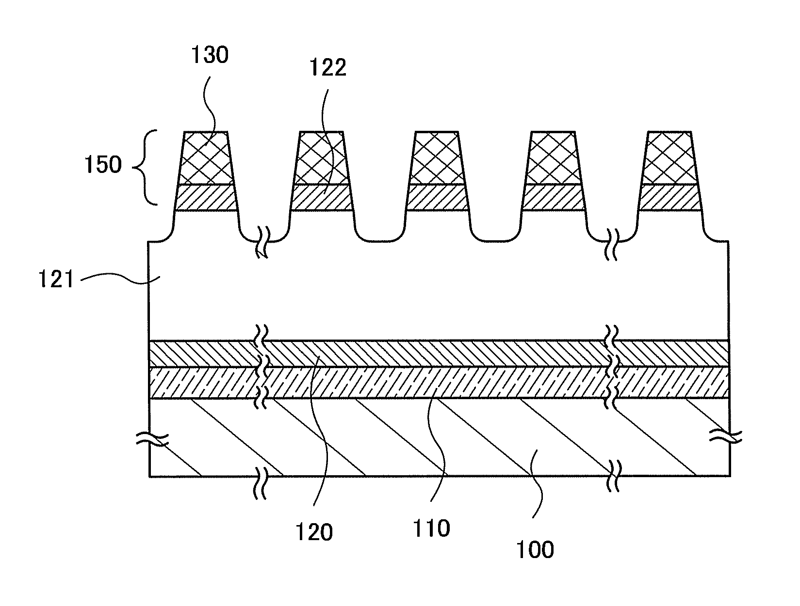
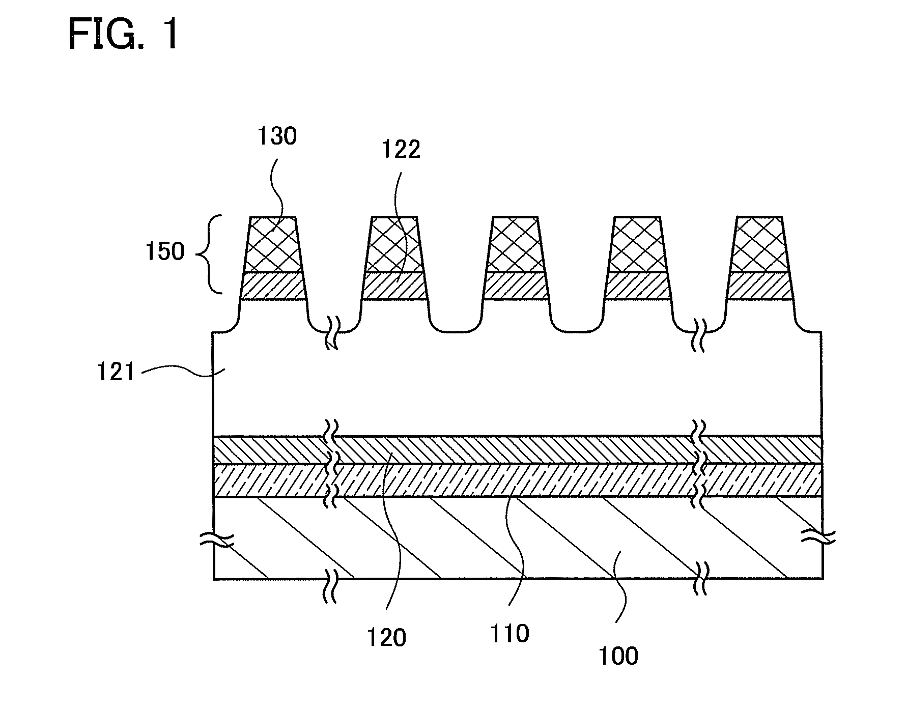
[0034]One embodiment of the present invention is an nip or pin type non-single-crystal thin film photoelectric conversion device in which a light-transmitting conductive film and an impurity semiconductor layer which have an opening are formed over an intrinsic semiconductor layer. In addition, the thickness of the intrinsic semiconductor layer under the opening is smaller than that of the intrinsic semiconductor layer under the light-transmitting conductive film and the impurity semiconductor layer.

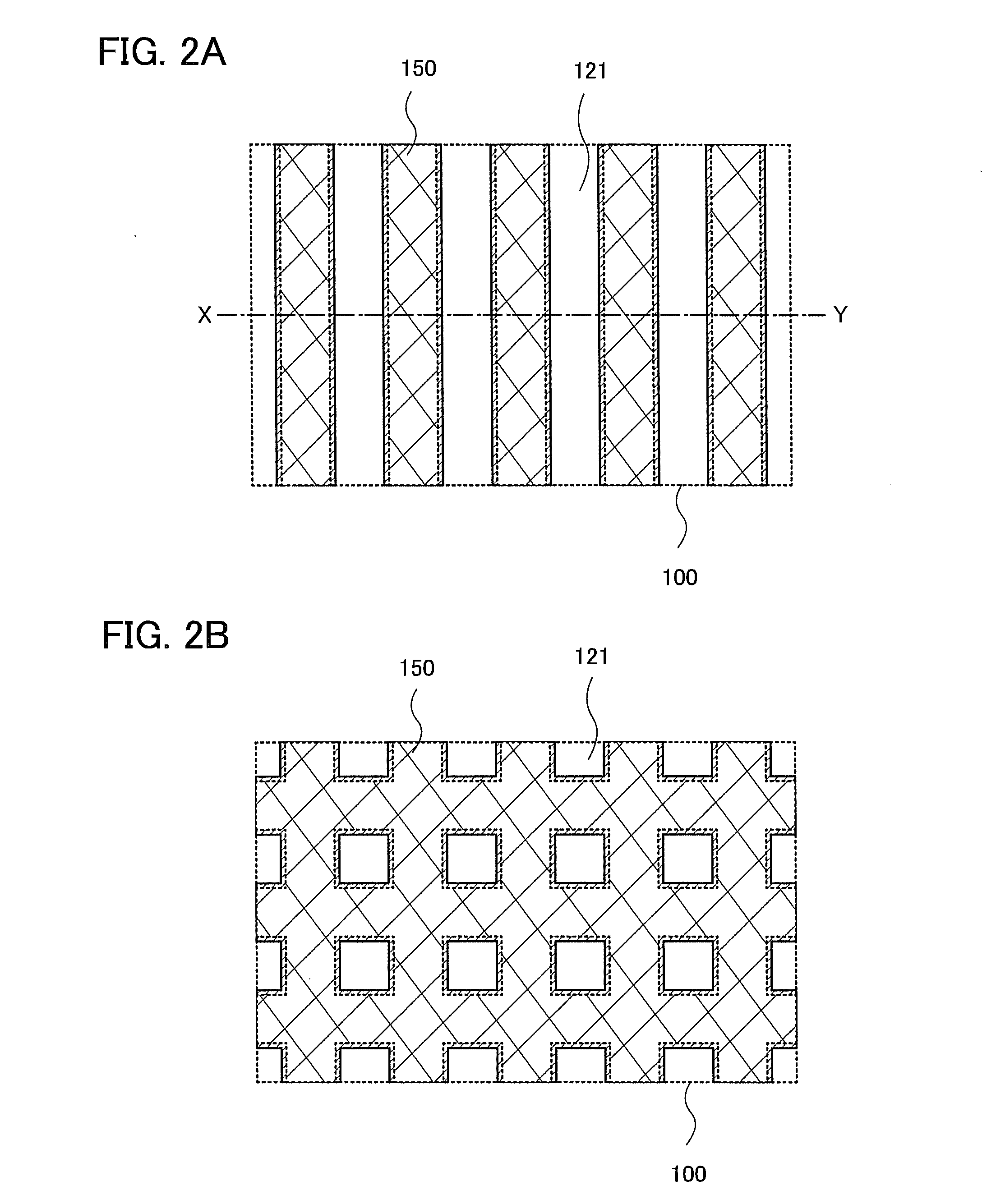
[0035]The structure of the photoelectric conversion device according to one embodiment of the present invention will be described. The photoelectric conversion device according to one embodiment of the present invention has, as is shown in the cross-sectional view of FIG. 1, a first electrode 110, a first impurity semiconductor layer 120, an intrinsic semiconductor layer 121, a second impurity semiconductor layer 122, and a second electrode 130 over an insulator 100. Hereinaf...

Example

Embodiment 2

[0062]In this embodiment, an example of a method for manufacturing the photoelectric conversion device according to one embodiment of the present invention will be described in detail with reference to drawings. Note that a description of the same parts as those of the above embodiment is omitted or partly simplified.

[0063]First, the first electrode 110 is formed over the insulator 100 (see FIG. 3A).

[0064]For the insulator 100, any insulator that can withstand a manufacturing process of the photoelectric conversion device according to the present invention can be used without particular limitation. A substrate having an insulating surface or an insulating substrate can be used. A glass substrate is preferably used because a large substrate can be obtained and cost can be reduced. For example, large substrates distributed as glass substrates for liquid crystal displays which have a size of 300 mm×400 mm of the first generation, 550 mm×650 mm of the third generation, 730 m...

Example

Embodiment 3

[0094]In this embodiment, an integration method for a photoelectric conversion device according to one embodiment of the present invention is described in detail with reference to drawings. Note that a description of the same parts as those of the above embodiment is omitted or partly simplified.

[0095]FIG. 6A is a plan view of the integrated photoelectric conversion device of this embodiment. FIGS. 6B and 6C are cross-sectional views taken along lines A-A′ and B-B′ in FIG. 6A, respectively. Although an example where two isolated cells are series connected for integration is shown in this embodiment, more cells can be integrated in order to obtain desired voltage.

[0096]In a usual nip thin film photoelectric conversion device, if steps up to the formation of the second electrode 130 are consecutively performed, integration would be difficult in terms of the structure. Therefore, a conductive film is formed after an element isolation step. In such a case where the film-form...


PUM


Abstract

A stack including a first electrode, a first impurity semiconductor layer having one conductivity type, an intrinsic semiconductor layer, a second impurity semiconductor layer having an opposite conductivity type to the one conductivity type, and a light-transmitting second electrode is formed over an insulator. The light-transmitting second electrode and the second impurity semiconductor layer have one or more openings. The shortest distance between one portion of the wall of one opening and an opposite portion of the wall of the same opening at the level of the interface between the second impurity semiconductor layer and the intrinsic semiconductor layer is made smaller than the diffusion length of holes in the intrinsic semiconductor layer. Thus, recombination is suppressed, so that more photocarriers are generated due to the openings and taken out as current, whereby conversion efficiency is increased.

Description

TECHNICAL FIELD[0001]The present invention relates to a photoelectric conversion device and a manufacturing method thereof.BACKGROUND ART[0002]Global warming has become a serious problem, and energy sources which will replace fossil fuels have been attracting increasing attention. In recent years, research and development on photoelectric conversion devices, which are also called solar cells, have become very active, and the market is rapidly expanding.[0003]The photoelectric conversion devices are attractive power generation means which use inexhaustible sunlight as the energy source and which do not emit carbon dioxide at the time of power generation. However, there are problems under present conditions in that photoelectric conversion efficiency per unit area is not sufficient, that the amount of power generation is affected by the daylight hours, and the like. Accordingly, a long time of around 20 years is needed for recovery of the initial cost. These problems prevent the wides...

Claims


Application Information

Patent Timeline
IPC IPC(8): H01L31/105H01L31/18
CPCH01L31/022433H01L31/02363H01L31/035281H01L31/046H01L31/202Y02E10/548H01L31/075H01L31/0463H01L31/0465Y02P70/50
Inventor NISHI, KAZUOKUSUMOTO, NAOTO
Owner SEMICON ENERGY LAB CO LTD
Why Eureka
Try Eureka