Silicon-based heterojunction solar cell and manufacturing method thereof

A technology of solar cells and manufacturing methods, applied in circuits, photovoltaic power generation, electrical components, etc., can solve the problems of unreachable roughness, weak hydrogen plasma resistance, and scarce indium ore, so as to improve photoelectric conversion efficiency and increase light The effect of absorbing and increasing the output current density

Inactive Publication Date: 2017-09-22
盐城金合盛光电科技有限公司
View PDF14 Cites 0 Cited by
  • Summary
  • Abstract
  • Description
  • Claims
  • Application Information

AI Technical Summary

Problems solved by technology

[0009] For transparent conductive films used in solar cells, indium tin oxide (ITO) has always been the mainstream material. However, indium ore is scarce and expensive, and its resistance to hydrogen plasma is weak. Therefore, it is necessary to develop alternative materials in the future.
However, the transparent conductive film deposited by the sputtering method disclosed in the above patent is too flat to achieve the required roughness and form a textured structure, so an additional etching process of the film must be performed, resulting in an increase in the manufacturing cost of the solar cell

Method used


Image

  • Silicon-based heterojunction solar cell and manufacturing method thereof
  • Silicon-based heterojunction solar cell and manufacturing method thereof
  • Silicon-based heterojunction solar cell and manufacturing method thereof

Examples


Embodiment Construction

[0068] While the present invention may be embodied in various forms, the drawings and description below are of preferred embodiments of the invention, and it is to be understood that what is disclosed herein is considered an example of the invention and is not intended to It is intended to limit the invention to the drawings and / or the specific embodiments described.

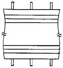
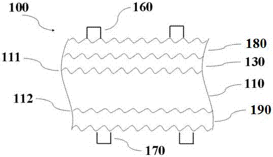
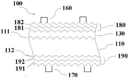
[0069] now please refer to figure 2 , which is shown as a structure of a silicon-based heterojunction solar cell 100 disclosed in the first embodiment of the present invention, which includes: a substrate 110; a semiconductor layer 130; a first transparent conductive film 180; a first electrode 160 ; a second transparent conductive film 190 ; and a second electrode 170 .

[0070] The substrate 110 is selected from one of a P-type semiconductor substrate, an N-type semiconductor substrate, a P-type silicon substrate, and an N-type silicon substrate. Preferably, the substrate 110 is selected from N-type semicon...


PUM

PropertyMeasurementUnit
Grain sizeaaaaaaaaaa
Surface roughnessaaaaaaaaaa

Abstract

The invention discloses a silicon-based heterojunction solar cell and a manufacturing method thereof. The silicon-based heterojunction solar cell comprises a silicon-based PN-junction structure, a first transparent conductive film, a second transparent conductive film, a first electrode and a second electrode. The transparent conductive films are rapidly deposited through electro-spraying cracking so that the silicon-based heterojunction solar cell has the characteristics of improving the current characteristic and enhancing the photoelectric conversion efficiency and can achieve rapid batch production.

Description

technical field [0001] The invention relates to a silicon-based heterojunction solar cell, in particular to a silicon-based heterojunction solar cell with a transparent conductive film deposited by electrospray cracking and a manufacturing method thereof. Background technique [0002] At present, due to the current international energy shortage, countries all over the world have been continuously researching and developing various alternative energy sources, and among them, solar cells that generate electricity from solar energy have attracted the most attention. At present, the conversion efficiency of solar cells made of silicon crystals is limited by the fact that they can only absorb sunlight above 1.1 electron volts (eV), the loss caused by reflected light, the material's insufficient ability to absorb sunlight, and the carrier Many factors, such as being captured by defects in the material and failing before being exported, or being recombined by carriers captured by s...

Claims


Application Information

Patent Timeline
IPC IPC(8): H01L31/0216H01L31/0224H01L31/072H01L31/18
CPCH01L31/02168H01L31/0224H01L31/072H01L31/18Y02E10/50Y02P70/50
Inventor 张金隆杨茹媛苏盛隆陈坤贤
Owner 盐城金合盛光电科技有限公司
Why Eureka
Try Eureka