Manufacturing method of OLED display panel and OLED display panel

A technology for a display panel and a manufacturing method, which is applied in the manufacture of semiconductor/solid-state devices, electrical components, and electrical solid-state devices, etc., can solve the problems of the conduction barrier between the cathode and the auxiliary electrode, the high impedance of the material, and the effect of affecting the voltage drop improvement.

Active Publication Date: 2019-08-16
SHENZHEN CHINA STAR OPTOELECTRONICS SEMICON DISPLAY TECH CO LTD
View PDF5 Cites 6 Cited by
  • Summary
  • Abstract
  • Description
  • Claims
  • Application Information

AI Technical Summary

Problems solved by technology

[0005] With the development of display technology, the size of the display panel is getting larger and larger, the size of the cathode of the OLED display panel is getting larger and larger, and the resistance of the cathode is also increasing accordingly, resulting in the voltage applied to the cathode being lower than the target value, resulting in a voltage For this reason, the prior art proposes a technical scheme of setting an auxiliary electrode on the same layer as the anode under the cathode, and connecting the cathode and the auxiliary electrode through an opening (Contact hole), which can effectively reduce the sheet resistance to improve the

Method used


Image

  • Manufacturing method of OLED display panel and OLED display panel
  • Manufacturing method of OLED display panel and OLED display panel
  • Manufacturing method of OLED display panel and OLED display panel

Examples


Embodiment Construction

[0040] In order to further illustrate the technical means adopted by the present invention and its effects, the following describes in detail in conjunction with preferred embodiments of the present invention and accompanying drawings.

[0041] see Figure 7 , the invention provides a method for manufacturing an OLED display panel, comprising the following steps:

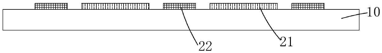
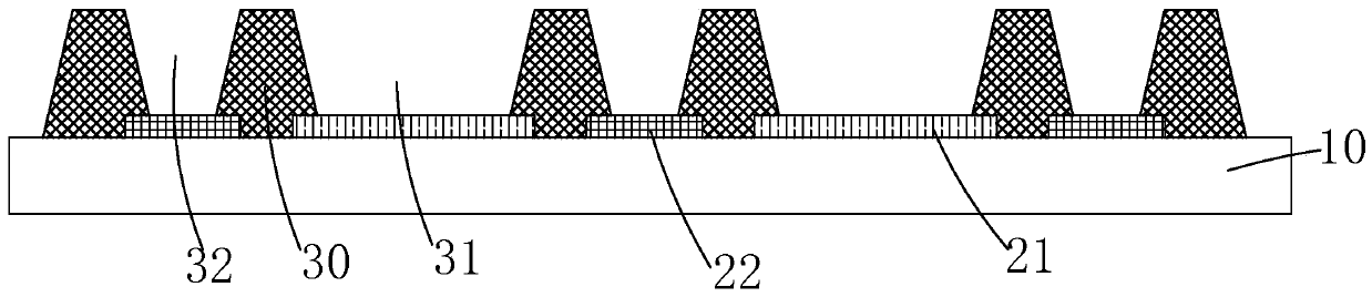
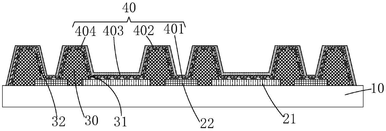
[0042] Step S1, please refer to figure 1 A base substrate 10 is provided, on which a plurality of anodes 21 arranged in an array and auxiliary electrodes 22 located in interval regions of the plurality of anodes 21 are formed.

[0043] Specifically, the base substrate 10 is a TFT substrate, on which a TFT array and a planar layer covering the TFT array are formed, and the plurality of anodes 21 and auxiliary electrodes 22 are all formed on the planar layer.

[0044] Specifically, in some embodiments of the present invention, the material of the anode 21 is transparent oxide, preferably indium tin oxide. Can be me...


PUM


Abstract

The invention provides a manufacturing method of an OLED display panel and the OLED display panel. The method comprises the steps: providing an underlying substrate and forming multiple anodes arranged in an array on the substrate and auxiliary electrodes arranged in spaced regions of multipl anodes; forming a pixel definition layer on the underlying substrate, multiple anodes and auxiliary electrodes and forming multiple first openings corresponding to multiple anodes and second openings corresponding to the auxiliary electrodes on the pixel definition layer; forming an OLED light emitting layer covering the whole surface on the auxiliary electrodes, the pixel defining layer and multiple anodes; performing UV illumination on the OLED light emitting layer; and forming a cathode distributedon the whole surface on the OLED light emitting layer. The current conductivity of the electron transmission material in the OLED light emitting layer can be improved by the UV illumination treatment, the conduction obstacle between the auxiliary electrodes and the cathode can be eliminated and the improvement effect of the voltage drop can be improved.

Description

technical field [0001] The invention relates to the field of display technology, in particular to a method for manufacturing an OLED display panel and the OLED display panel. Background technique [0002] Organic Light Emitting Display (OLED) has self-illumination, low driving voltage, high luminous efficiency, short response time, high definition and contrast, nearly 180° viewing angle, wide operating temperature range, and can realize flexible display and With many advantages such as large-area full-color display, it is recognized by the industry as a display device with the most potential for development. [0003] According to the driving method, OLED can be divided into two categories: passive matrix OLED (Passive Matrix OLED, PMOLED) and active matrix OLED (Active Matrix OLED, AMOLED), namely direct addressing and thin film transistor matrix addressing. Among them, AMOLED has pixels arranged in an array, belongs to the active display type, has high luminous efficiency,...

Claims


Application Information

Patent Timeline
IPC IPC(8): H01L51/50H01L51/56
CPCH10K71/00H10K50/16H10K50/11
Inventor 杜中辉吴元均
Owner SHENZHEN CHINA STAR OPTOELECTRONICS SEMICON DISPLAY TECH CO LTD
Why Eureka
Try Eureka