Millimeter wave active antenna unit and inter-PCB (Printed Circuit Board) interconnection structure

A technology of PCB board and interconnection structure, applied in the field of millimeter wave active antenna unit and interconnection structure between PCB boards, can solve the problems of high cost, low suitable frequency, and small number of stacks, etc.

Pending Publication Date: 2019-08-23
COMBA TELECOM SYST CHINA LTD
View PDF0 Cites 18 Cited by
  • Summary
  • Abstract
  • Description
  • Claims
  • Application Information

AI Technical Summary

Problems solved by technology

However, the traditional AIP antenna module usually adopts BGA ball planting method to complete the inter-board interconnection design, so the cost is high, or the millimeter-wave AAU product obtained by PCB board welding process is low in cost, but it is suitable for relatively low frequency , When the number of layers is relatively small

Method used


Image

  • Millimeter wave active antenna unit and inter-PCB (Printed Circuit Board) interconnection structure
  • Millimeter wave active antenna unit and inter-PCB (Printed Circuit Board) interconnection structure
  • Millimeter wave active antenna unit and inter-PCB (Printed Circuit Board) interconnection structure

Examples


Embodiment Construction

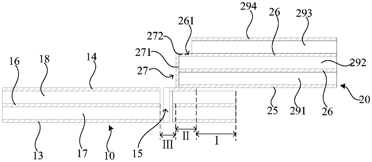
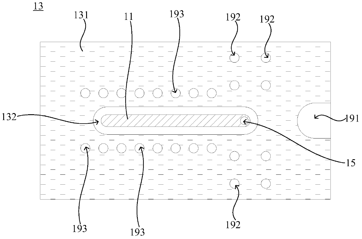
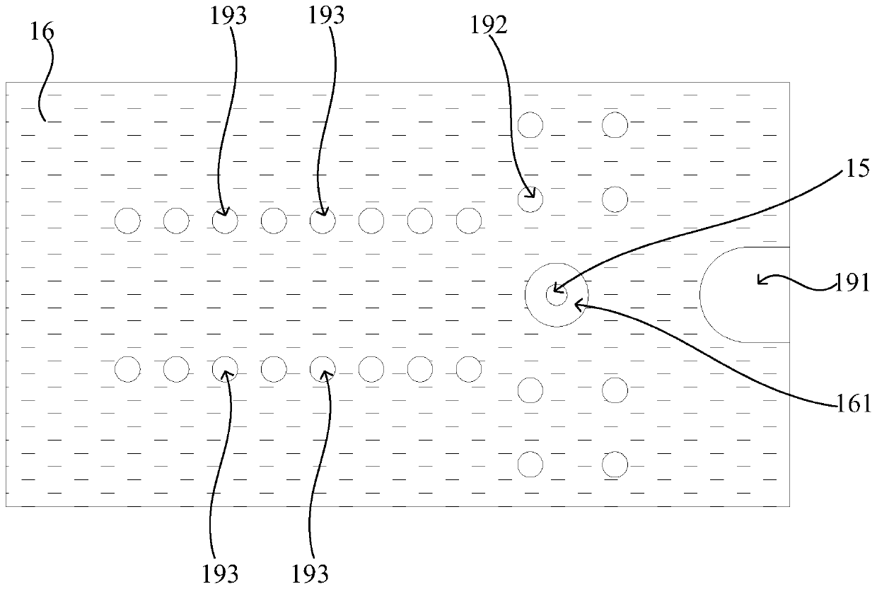
[0035] In order to make the above objects, features and advantages of the present invention more comprehensible, specific implementations of the present invention will be described in detail below in conjunction with the accompanying drawings. In the following description, numerous specific details are set forth in order to provide a thorough understanding of the present invention. However, the present invention can be implemented in many other ways different from those described here, and those skilled in the art can make similar improvements without departing from the connotation of the present invention, so the present invention is not limited by the specific embodiments disclosed below.

[0036] In the description of the present invention, it should be understood that the terms "first" and "second" are used for description purposes only, and cannot be interpreted as indicating or implying relative importance or implicitly indicating the quantity of indicated technical featu...


PUM


Abstract

The invention relates to a millimeter wave active antenna unit and an inter-PCB (Printed Circuit Board) interconnection structure. The inter-PCB interconnection structure comprises a main board and anAIP (Antenna in package) antenna module. The main board is a first multilayer PCB and provided with a signal transmission line and a first pad electrically connected with the signal transmission line. The AIP antenna module is a second multilayer PCB and provided with a second pad, an impedance matching transmission branch, an impedance line and a signal processing circuit. The main board and theAIP antenna module adopts a mode of direct welding interconnection between the multilayer PCBs, thereby saving an expensive millimeter wave interconnection assembly on the one hand, and thus being very low in cost; On the other hand, the mode of direct welding between the boards improves the reliability of the product, the interconnection design between the multilayer PCBs can be realized, and the integration between the multilayer PCBs is greatly improved, thereby being conducive to the miniaturization design of millimeter wave equipment. In addition, the second pad and the signal processingcircuit are provided with the impedance matching transformation branch and the impedance line therebetween, thereby being suitable for a wider frequency range and a wider lamination number range.

Description

technical field [0001] The invention relates to the technical field of millimeter wave communication, in particular to a millimeter wave active antenna unit and an interconnection structure between PCB boards. Background technique [0002] With the development of 5G communication technology, millimeter wave has significant advantages in large bandwidth and high-speed communication. The 5G system requires overall planning and complementary advantages of Sub-6GHz and millimeter wave frequency bands. 5G millimeter wave can be widely used in small base stations, CPE (customer premise equipment, customer premise equipment), Repeater (repeater) and other scenarios. The millimeter-wave AAU (Active Antenna Unit, active antenna unit) products include an AIP (Antenna in package, antenna in package) antenna module and a motherboard connected to the AIP antenna module. The antenna radiating unit of the AIP antenna module is located on the surface layer of the multilayer PCB (multilaye...

Claims


Application Information

Patent Timeline
Patent Type & Authority Applications(China)
IPC IPC(8): H05K1/14H05K1/11
CPCH05K1/141H05K1/117H05K1/025H05K1/0251H05K2201/041H05K2201/09727H05K2201/09618H05K2201/09181H01Q1/2283H01P5/028H01P1/047H01Q5/335H01Q1/424H01Q13/08
Inventor 高永振伍尚坤张志梅高霞钟伟东
Owner COMBA TELECOM SYST CHINA LTD
Why Eureka
Try Eureka