Deep silicon etching method for MEMS

A technology of deep silicon etching and etching cavity, which is applied in the process of producing decorative surface effects, decorative art, gaseous chemical plating, etc., can solve the problem of high roughness of side walls of MEMS devices, uneven etching, cavity The problem of high temperature of the chamber and sample stage can be solved to reduce surface contamination and damage, improve performance and reliability, and provide uniformity

Active Publication Date: 2019-08-27
JIANGSU LEUVEN INSTR CO LTD
View PDF7 Cites 3 Cited by
  • Summary
  • Abstract
  • Description
  • Claims
  • Application Information

AI Technical Summary

Problems solved by technology

In the deep silicon etching system, if there are too many cycles in multiple steps, the temperature of the chamber and the sample stage will be too high, which will lead to uneven etching and excessive roughness of the side wall of the MEMS device.

Method used


Image

  • Deep silicon etching method for MEMS
  • Deep silicon etching method for MEMS
  • Deep silicon etching method for MEMS

Examples


Embodiment Construction

[0045] In order to clearly illustrate the technical features of the solution, the solution will be described below through specific implementation modes.

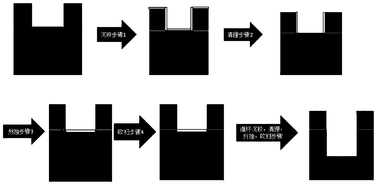
[0046] see Figure 1 to Figure 3 , the present invention is: a MEMS deep silicon etching method specifically includes the following content:

[0047] (1) Pretreatment steps of MEMS samples: the wafer is transferred from the transfer chamber to the vacuum reaction chamber, and a cycle of deposition steps, cleaning steps and etching steps are completed in the vacuum reaction chamber. After completing several cycles , the depth of silicon etching meets the requirements of MSMS devices, the MEMS devices are transferred from the vacuum reaction chamber to the transfer chamber, the wafer is returned to the atmosphere state, and the processing on the subsequent equipment is carried out; after the MEMS samples are subjected to the photolithography process, the The CD width of the photoresist is 50um, the line spacing is 40um, the ...


PUM


Abstract

The invention provides a deep silicon etching method for an MEMS, and belongs to the technical field of deep silicon etching. According to the technical scheme, the deep silicon etching method of theMEMS comprises a deposition step, a cleaning step, an etching step, a purging step, a repeated deposition step, a repeated cleaning step, a repeated etching step and a repeated purging step, and is characterized in that side circulation is carried out through the deposition step, the cleaning step, the etching step and the purging step for multiple times, and a sample is vacuumized. The beneficialeffects of the deep silicon etching method are as follows: the deep silicon etching method disclosed by the invention can be applied to a large-scale integrated circuit industrial manufacturing environment; particularly, the integrity of sensing elements can be kept during long-time etching, the device design requirement can be met, the purging step is added, the temperature of the vacuum reaction chamber and the temperature of the sample table can be reduced, the vacuum reaction chamber is kept within a constant range, and the uniformity of large-size samples after being etched and the roughness of the side wall of the MEMS device can be easily provided.

Description

technical field [0001] The invention relates to the technical field of deep silicon etching, in particular to a MEMS deep silicon etching method. Background technique [0002] Micro-electromechanical systems (MEMS) is the integration of information sensing, processing, mechanical execution and other micro-devices in a micro-system in a high-density, low-cost manner according to the manufacturing principles of integrated circuits. The interdisciplinary phenomenon in MEMS is extremely obvious, mainly involving micromachining technology, mechanics, solid acoustic theory, heat flow theory, electronics, biology, etc. The characteristic length is from 1um to 1mm. [0003] The processing technology for MEMS devices is not mechanical. Instead, they employ microfabrication techniques similar to batch processing of integrated circuits. Mass manufacturing can significantly reduce the cost of mass production. If the area of ​​a single MEMS sensor chip is 5mm*5mm, then an 8-inch (20 c...

Claims


Application Information

Patent Timeline
Patent Type & Authority Applications(China)
IPC IPC(8): B81C1/00
CPCB81C1/00531B81C1/00555B81C1/00619
Inventor 王珏斌许开东胡东东车东晨
Owner JIANGSU LEUVEN INSTR CO LTD
Why Eureka
Try Eureka