Patterned color conversion array Micro LED as well as preparation method and application thereof

A color conversion and patterning technology, applied in electrical components, electrical solid devices, circuits, etc., can solve the problems of uneven coating of phosphor powder, poor material stability, affecting display quality, etc., and achieve high mechanical strength and high performance. Good stability and color uniformity

Active Publication Date: 2019-08-27
XI AN JIAOTONG UNIV
View PDF5 Cites 0 Cited by
  • Summary
  • Abstract
  • Description
  • Claims
  • Application Information

AI Technical Summary

Problems solved by technology

Disadvantages of phosphor as a fluorescent material: the phosphor coating will absorb part of the energy and reduce the conversion rate; the size of the phosphor particles is large, and as the micro-LED pixel size continues to decrease, the phosphor coating becomes less and less Uniform and affects display quality
The disadvantages of quantum dots as fluorescent light-emitting materials: the uniformity of each color and the mutual influence between each color, poor material stability, high heat dissipation requirements, and need to be sealed, short life, etc.

Method used


Image

  • Patterned color conversion array Micro LED as well as preparation method and application thereof
  • Patterned color conversion array Micro LED as well as preparation method and application thereof
  • Patterned color conversion array Micro LED as well as preparation method and application thereof

Examples


Embodiment 1

[0052] A method for preparing a patterned color conversion array micro LED, comprising the following steps:

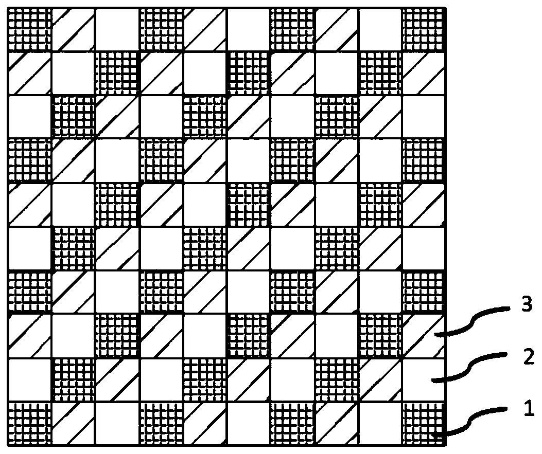
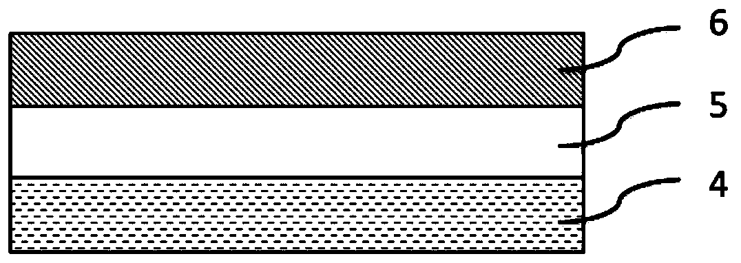
[0053] Step 1: Align the red fluorescent crystal 6 and the green fluorescent crystal 4 to be processed by bonding the intermediate layer 5 to carry out three-layer bonding. The cross-sectional view of the sample after bonding is shown in figure 2 , the bonded sample includes a green fluorescent crystal 4 , an adhesive intermediate layer 5 and a red fluorescent crystal 6 sequentially arranged from bottom to top. Among them, the adhesive middle layer is 3M TM Optically clear adhesive 8146-x;

[0054] Step 2: Cut off the redundant part of the periodic pattern of the red fluorescent crystal 6 by laser processing and cutting to form a number of red fluorescent crystal grains 3 , and make a period of the red fluorescent fluorescent crystal grain 3 on the side of the adhesive intermediate layer 5 sexual array.

[0055] In step 2, the patterns obtained by laser processing ...

Embodiment 2

[0059] The specific implementation steps of a method for preparing a patterned color conversion array micro LED are as follows:

[0060] Step 1: Bond the red fluorescent crystal 6 with a thickness of 2 mm and the green fluorescent crystal 4 with a thickness of 2 mm to be processed. For the cross-sectional view of the sample formed after bonding, see Figure 6 .

[0061] Step 2: cut off the redundant part 8 of the periodic pattern of the red fluorescent crystal 6 by laser processing and cutting to form a number of red fluorescent crystal grains 3 and a number of green fluorescent crystal grains 2 to obtain a periodic array.

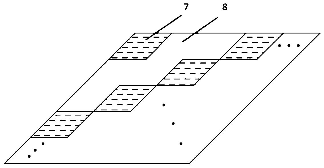
[0062] Wherein, cutting the red fluorescent crystal 6 keeps the frame. The red fluorescent crystal grains 3 are connected to each other, several green fluorescent crystal grains 2 and the first frame 91, and the edges of the red fluorescent crystal grains 3 are directly connected to the reserved frame, as Figure 7 shown.

[0063] Step 3: Turn over the ...

Embodiment example 3

[0066] The specific implementation steps of a method for preparing a patterned color conversion array micro LED are as follows:

[0067] Step 1: Process the red fluorescent crystal 6 and the green fluorescent crystal 4 by laser cutting to realize the patterning of the fluorescent crystal material, and respectively obtain the green fluorescent crystal grains 2 and the red fluorescent crystal grains 3 arranged in an array. After processing, the fluorescent crystal has a reserved frame, and the width of the reserved frame of the red fluorescent crystal is the same as that of the green fluorescent crystal. The patterns are connected to each other, and the edges are directly connected to the reserved frame, such as Figure 7 shown.

[0068] Step 2: Align the reserved frames of the patterned red fluorescent crystals and green fluorescent crystals up and down, such as Figure 8 shown.

[0069] Step 3: Double-layer bonding or triple-layer bonding (transparent bonding middle layer 5...


PUM


Abstract

The invention discloses a patterned color conversion array Micro LED as well as a preparation method and an application thereof, and provides a three-primary-color element display packaging structureformed by a combination of a red, green fluorescent single crystal or polycrystalline fluorescence conversion material and a Micro-LED blue light backlight source, so that the display of a colorful image is realized, the color gamut of a display screen can be effectively improved, and the color is more distinct. By adopting the structure, the process of manufacturing the display screen is simple,the packaging efficiency and the yield can be greatly improved, the production cost is reduced, and the service life of the display screen is prolonged. The problem that the resolution is limited dueto the fact that the size of a light-emitting unit of an LED in the existing LED micro-display is difficult to be small is solved.

Description

technical field [0001] The invention belongs to the technical field of micro LED colorization, and in particular relates to a patterned color conversion array Micro LED and its preparation method and application. Background technique [0002] The general LED grain size is between 200-300 microns, the Mini LED (called the predecessor of Micro LED) is about 50-60 microns, and the Micro LED is about 15-30 microns. Micro LED technology refers to a high-density micro-sized LED array integrated on a chip. These arrays often include red-LED, green-LED and blue-LED arrays. Each pixel is a Micro LED that contains these three colors. LED units, thereby reducing pixel size and distance from millimeters to microns. For example, each pixel of the LED display can be addressed and individually driven to light up, which can be regarded as a miniature version of the outdoor LED display. Micro LED has the characteristics of high efficiency, high brightness, high reliability, and fast respon...

Claims


Application Information

Patent Timeline
Patent Type & Authority Applications(China)
IPC IPC(8): H01L33/50H01L27/15
CPCH01L27/156H01L33/502H01L33/504H01L2933/0041
Inventor 李虞锋杜玮云峰
Owner XI AN JIAOTONG UNIV
Why Eureka
Try Eureka