Anti-adherence protection patch for electronic product package

A technology for electronic products and packaging. It is applied in the field of anti-adsorption protective stickers for electronic product packaging. It can solve the problems of adhesion and adsorption, unfavorable protection of electronic products, scratches, etc., achieve high peeling force, improve comprehensive performance, and prevent scratches. Effect

Inactive Publication Date: 2019-08-30
SUZHOU SIDIKE NEW MATERIALS SCI & TECH
View PDF5 Cites 0 Cited by
  • Summary
  • Abstract
  • Description
  • Claims
  • Application Information

AI Technical Summary

Problems solved by technology

Due to the inherent particularity of electronic products, electronic product packaging materials need to have basic properties such as anti-static, moisture-proof, and impact resistance. However, the existing electronic product packaging materials still have scratches, electrostatic adsorption, adhesion and adsorption after long-term transportation and wear. A series of problems, which is not conducive to the protection of electronic products themselves

Method used


Image

  • Anti-adherence protection patch for electronic product package
  • Anti-adherence protection patch for electronic product package
  • Anti-adherence protection patch for electronic product package

Examples


Embodiment 1

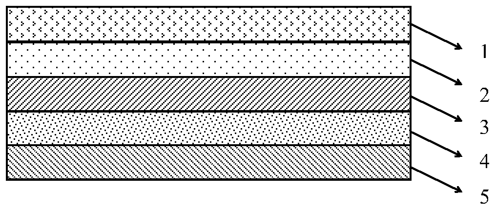
[0024] Embodiment 1: An anti-adsorption type protective sheet for electronic product packaging, the anti-adsorption type protective sheet includes an HC layer, an OCA layer, an optical PET layer, a silica gel layer and a release film laminated sequentially from top to bottom.

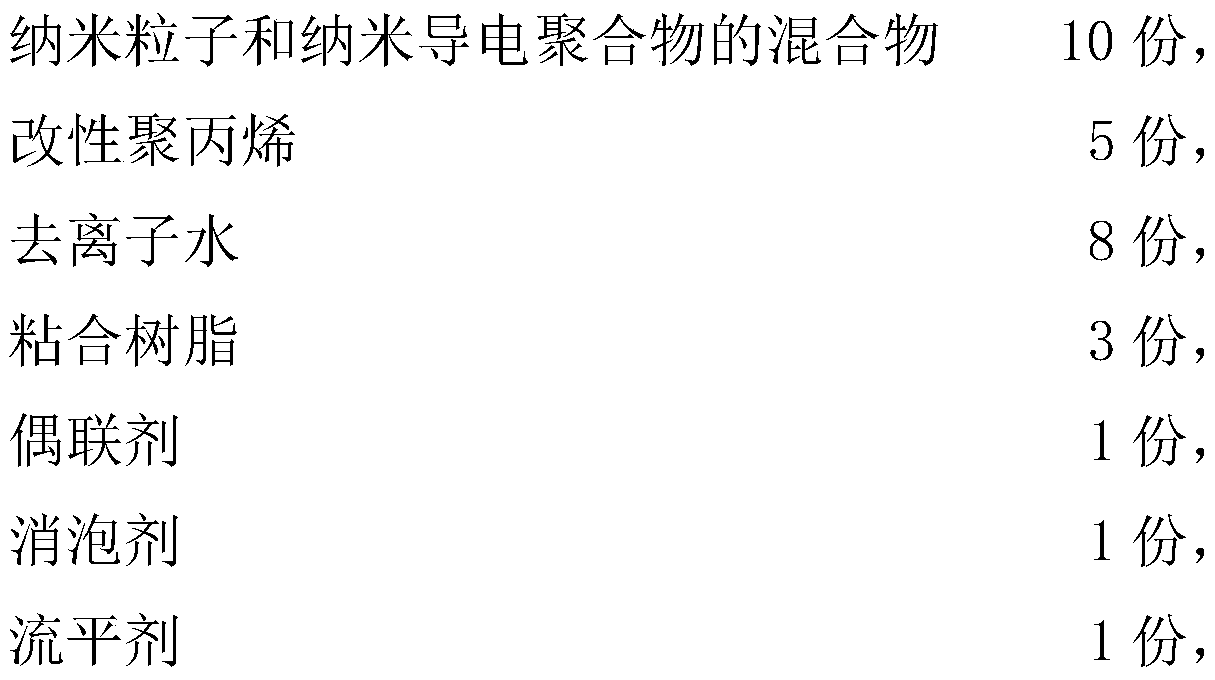
[0025] The HC layer includes the following components by weight: 80 parts of wear-resistant resin, 1 part of antistatic agent, 1 part of softener, 3 parts of curing agent, 50 parts of solvent, and 1 part of nano silicon dioxide.

[0026] Wherein, the antistatic agent includes the following components in the above-mentioned corresponding parts by weight:

[0027]

[0028] Wherein, the mass ratio of the nanoparticles to the nanoconductive polymer is 3:10, the nanoparticles are titanium oxide, the nanoconductive polymer is polyaniline, and the modified polypropylene is carbon fiber modified polypropylene, The adhesive resin is melamine formaldehyde resin, the coupling agent is silane coupling agent kh57...

Embodiment 2

[0031] An anti-absorption type protective sticker for electronic product packaging, the anti-absorption type protective sticker includes an HC layer, an OCA layer, an optical PET layer, a silica gel layer and a release film laminated sequentially from top to bottom.

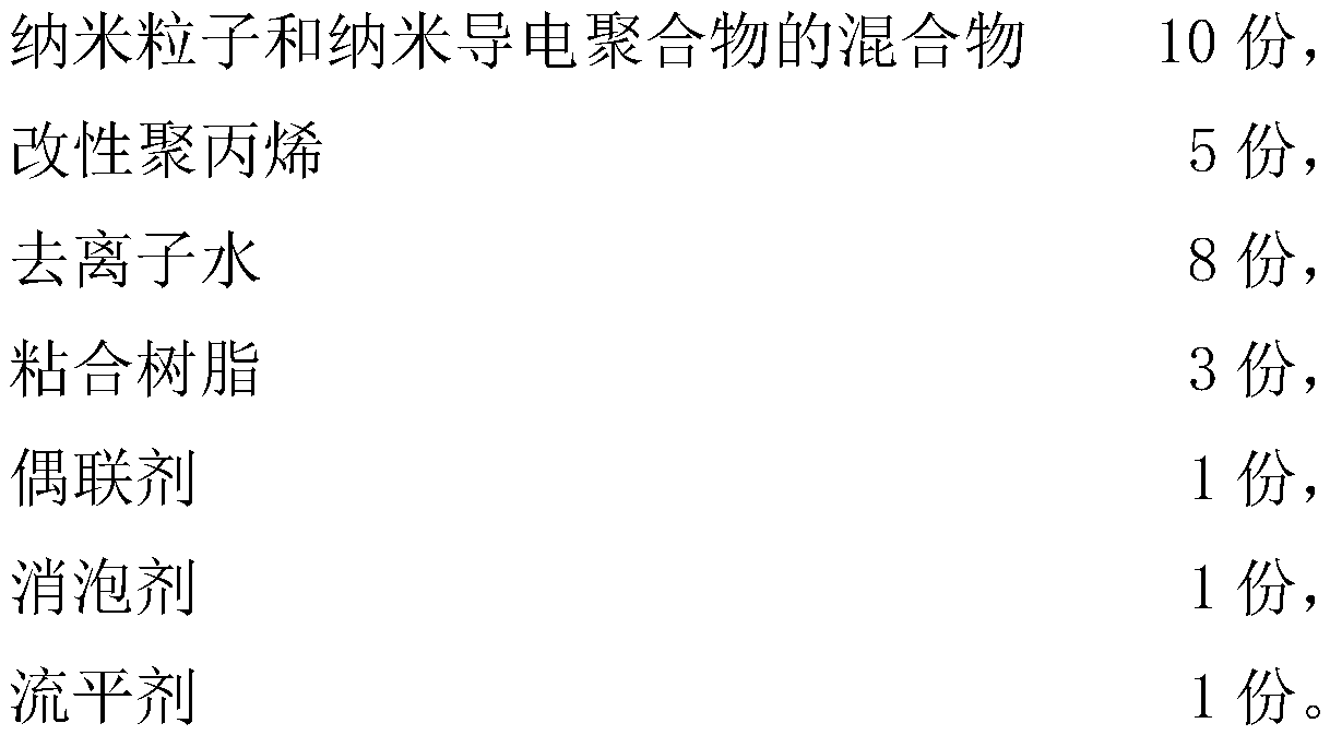
[0032] The HC layer includes the following components by weight: 80 parts of wear-resistant resin, 1 part of antistatic agent, 1 part of softening agent, 3 parts of curing agent, 50 parts of solvent, 1 part of nano silicon dioxide, the antistatic agent Parts by weight include the following ingredients:

[0033]

[0034] Wherein, the mass ratio of the nanoparticles to the nano-conducting polymer is 3:10, the nanoparticles are zinc oxide, the nano-conducting polymer is polytrimethylthiophene, and the modified polypropylene is asbestos-modified Polypropylene, the adhesive resin is LLDPE adhesive resin, the coupling agent is silane coupling agent kh792, the defoamer is phenylethyl alcohol oleate, and the leveling ...

Embodiment 3

[0037] An anti-absorption type protective sticker for electronic product packaging, the anti-absorption type protective sticker includes an HC layer, an OCA layer, an optical PET layer, a silica gel layer and a release film laminated sequentially from top to bottom.

[0038] The HC layer includes the following components by weight: 100 parts of wear-resistant resin, 3 parts of antistatic agent, 5 parts of softening agent, 6 parts of curing agent, 100 parts of solvent, 13 parts of nano silicon dioxide, the antistatic agent Parts by weight include the following ingredients:

[0039]

[0040] Wherein, the mass ratio of the nanoparticles to the nanoconductive polymer is 4:9, the nanoparticles are titanium oxide, the nanoconductive polymer is polyaniline, and the modified polypropylene is glass-reinforced polypropylene, so The adhesive resin is melamine formaldehyde resin, the coupling agent is silane coupling agent kh570, the defoamer is tributyl phosphate, and the leveling age...


PUM


Abstract

The invention discloses an anti-adherence protection patch for electronic product package. The patch comprises an HC (Hydrocarbon Compound) layer, an OCA (Optically Clear Adhesive) layer, an optical PET (Polyethylene Glycol Terephthalate) layer, a silica gel layer and a release membrane which are arranged in sequence. The anti-adherence protection patch has high permeability and haze, problems that a conventional protection patch for electronic product package has long-term transportation abrasion, scratching damage caused in use, electrostatic adherence, and the like, can be solved, the problem that a common HC is adhered to a packaging box since a surface is particularly flat can be avoided because of a designed planar microcosmic concave-convex structure, meanwhile, the flexibility of the protection patch can be improved, then the patch can be easily fitted with an electronic product with radians or curved surfaces, and in addition, the silica gel layer is easy in adherence and goodin bubble elimination effect and can be repeatedly used.

Description

technical field [0001] The invention relates to the field of electronic product packaging, in particular to an anti-adsorption protective sticker for electronic product packaging. Background technique [0002] With the progress of science and technology and the development of society, electronic products are becoming more and more popular and become an indispensable part of our daily life. Due to the inherent particularity of electronic products, electronic product packaging materials need to have basic properties such as anti-static, moisture-proof, and impact resistance. However, the existing electronic product packaging materials still have scratches, electrostatic adsorption, adhesion and adsorption after long-term transportation and wear. A series of problems are not conducive to the protection of electronic products themselves. In order to solve the above problems, it is urgent to provide a protective material for electronic product packaging with good properties such...

Claims


Application Information

Patent Timeline
Patent Type & Authority Applications(China)
IPC IPC(8): C09J7/29C08L79/02C08L63/00C08L23/12C08L65/00C08L61/28C08L23/08C08K13/04C08K3/22C08K7/06C08K7/12C08K7/14
CPCC08K2003/2241C08K2003/2296C08K2201/011C08L63/00C08L75/04C08L2201/04C08L2205/025C08L2205/035C09J7/29C09J2203/326C09J2301/122C09J2301/16C09J2463/006C09J2467/006C09J2475/006C09J2483/00C08L79/02C08L23/12C08L61/28C08K13/04C08K3/22C08K7/06C08L65/00C08L23/0815C08K7/12
Inventor 金闯张庆杰
Owner SUZHOU SIDIKE NEW MATERIALS SCI & TECH
Why Eureka
Try Eureka