Molybdenum disulfide/Sn co-doping composite film on base body surface and preparing method thereof
A technology of molybdenum disulfide and composite thin film, applied in ion implantation plating, metal material coating process, coating, etc., can solve the problems of reduced wear resistance, loss of lubrication effect, etc., and achieve the effect of improving the bonding force of the film base
- Summary
- Abstract
- Description
- Claims
- Application Information
AI Technical Summary
Problems solved by technology
Method used
Image
Examples
Embodiment 1
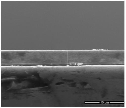
[0045] In this embodiment, the substrate material is 304 stainless steel, and the composite film on the surface of the substrate has a multi-layer structure, and its composition is: from the surface of the substrate along the thickness direction: a Ti transition layer with a thickness of 200nm, a Ti transition layer with a thickness of 50nm and MoS 2 A gradient transition layer with a thickness of 3.5 μm in MoS 2 Floor.
[0046] The composite film is prepared by magnetron sputtering technology, which mainly includes the following steps:
[0047] (1) Perform mechanical polishing on the surface of the substrate, put the substrate material in an acetone solution for 30 minutes of ultrasonic cleaning, blow dry with nitrogen, put it in absolute ethanol solution for 30 minutes of ultrasonic cleaning, blow dry with nitrogen and take it out.
[0048] (2) Put the substrate cleaned in step (1) into the magnetron sputtering chamber, and vacuum the chamber until the vacuum degree is low...
Embodiment 2
[0054] In this embodiment, the substrate material is 304 stainless steel, and the composite film on the surface of the substrate has a multi-layer structure. From the surface of the substrate along the thickness direction, its composition is as follows: Ti bonding layer with a thickness of 200nm, Ti and MoS with a thickness of 50nm. 2 Gradient transition layer with Sn, MoS with a thickness of 3.5 μm 2 Co-doped layer with Sn. In this embodiment, the atomic percentage of Sn in the composite film is 1.8%.
[0055] The composite film is prepared by magnetron sputtering technology, which mainly includes the following steps:
[0056] (1) Perform mechanical polishing on the surface of the substrate, put the substrate material in an acetone solution for 30 minutes of ultrasonic cleaning, blow dry with nitrogen, put it in absolute ethanol solution for 30 minutes of ultrasonic cleaning, blow dry with nitrogen and take it out.
[0057] (2) Put the substrate cleaned in step (1) into the...
Embodiment 3
[0063] In this embodiment, the matrix and the composite film on the surface of the matrix are basically the same as in Example 1, except that the atomic percentage of Sn in the composite film is 2.5%.
[0064] In the present embodiment, the preparation method of the composite film is basically the same as in Example 1, except that steps (3-2) and (3-3) are as follows:
[0065] (3-2) Enable MoS 2 target sputtering current, and gradually increase the MoS 2 Target sputtering current to 1.6A; at the same time, turn on the Sn target sputtering current, and gradually increase the Sn target sputtering current to 0.4A; at the same time, gradually reduce the Ti target sputtering current to 0A, and the working pressure is 0.1-1.0Pa , the bias voltage is -30~-70V, and the gradient transition layer is deposited on the surface of the Ti bonding layer;
[0066] (3-3) Keep MoS 2 The target sputtering current was 1.6A, the Sn target sputtering current was 0.4A respectively, and the co-dope...
PUM
| Property | Measurement | Unit |
|---|---|---|
| thickness | aaaaa | aaaaa |
| thickness | aaaaa | aaaaa |
| thickness | aaaaa | aaaaa |
Abstract
Description
Claims
Application Information


