Method for preparing beta-Ga2O3 film

A -ga2o3 thin film technology, applied in the field of preparation of β-Ga2O3 thin film, can solve the problems that cannot be obtained and affect the performance of optoelectronic devices, etc.

Active Publication Date: 2019-09-03
BEIJING UNIV OF TECH
View PDF3 Cites 14 Cited by
  • Summary
  • Abstract
  • Description
  • Claims
  • Application Information

AI Technical Summary

Problems solved by technology

However, the Ga deposited by this method 2 o 3 The film is in a metastable state and is easily converted to polycrystalline form Ga 2 o 3 , the expected β-Ga 2 o 3 single crystal, which in turn affects β-Ga-based 2 o 3 The performance of optoelectronic devices

Method used


Image

  • Method for preparing beta-Ga2O3 film
  • Method for preparing beta-Ga2O3 film
  • Method for preparing beta-Ga2O3 film

Examples


Embodiment Construction

[0023] The technical solution of the present invention will be described more clearly and completely below in conjunction with the accompanying drawings. Any modification or equivalent replacement of the technical solution of the present invention without departing from the scope of the technical solution of the present invention shall be covered within the protection scope of the present invention.

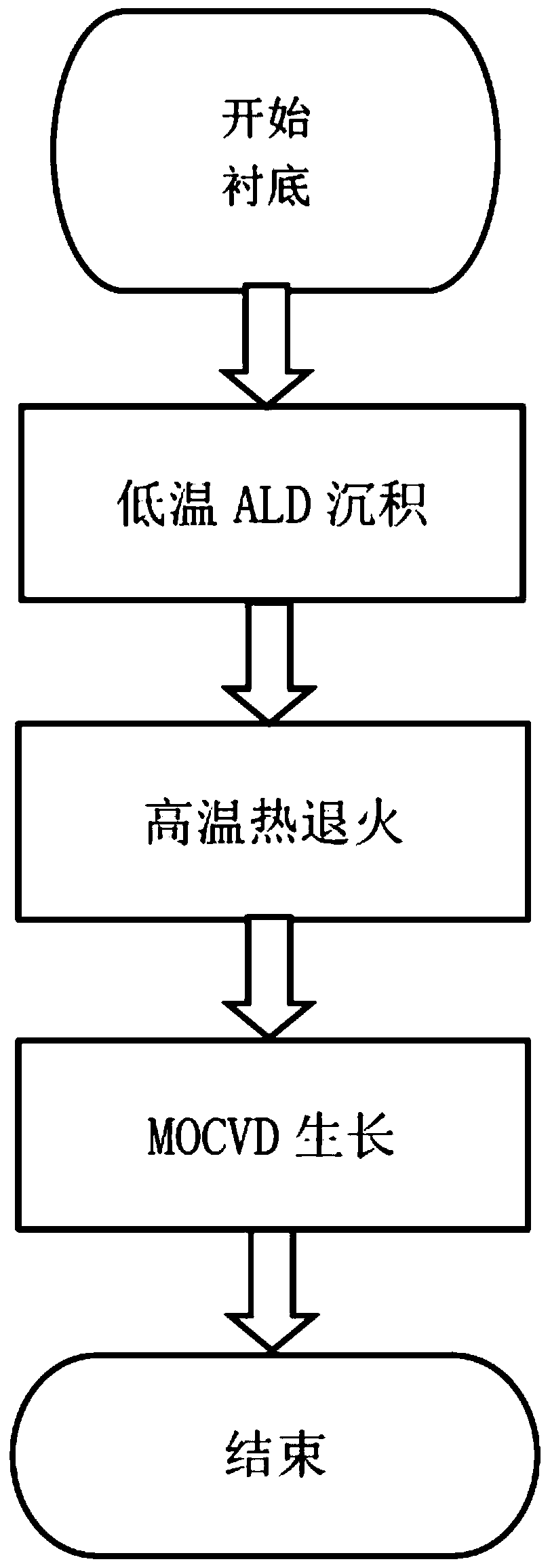
[0024] The specific implementation steps include:

[0025] (1) Select the (0001) plane sapphire substrate; use plasma-enhanced atomic layer deposition to grow Ga on sapphire 2 o 3 For thin film, the RF plasma power is 2000W, the substrate is heated to a constant temperature of 250°C, and nitrogen is used as the carrier gas;

[0026] (2) Plasma-enhanced atomic layer deposition is as follows: ①Then pass into the TMGa source for 0.1s, and the TMGa flow rate is 200sccm; ②Then pass through the nitrogen gas for 5s; Nitrogen for 5s; ⑤Then cycle 420 cycles from step ① to step ④ and ent...


PUM

PropertyMeasurementUnit
transmittivityaaaaaaaaaa

Abstract

The invention provides a method for preparing beta-Ga2O3 film and belongs to the technical field of micro-electronics. The problems of phase mixing and poor crystalline quality during preparation of the beta-Ga2O3 film are solved. The method comprises the steps that atomic layer deposition is reinforced through plasma, Ga2O3 film is grown on sapphire substrate, then high-temperature annealing recrystallization is conducted, metastable Ga2O3 is converted into stable Ga2O3, and finally the beta-Ga2O3 film is grown through metal organic chemical vapor deposition technology. The method for preparing the single-phase beta-Ga2O3 film can lay the foundation for preparing thick beta-Ga2O3 materials and devices.

Description

technical field [0001] The invention belongs to the field of microelectronic technology, relates to the field of semiconductor material science and technology, in particular to a method for preparing β-Ga 2 o 3 Thin film method. Background technique [0002] After the wide-bandgap semiconductor material SiC / GaN, ultra-wide bandgap (UWB) semiconductor is an emerging semiconductor, and its operating temperature and power are much higher than traditional small-bandgap Si-based chips. Therefore, ultra-wide bandgap (UWB) semiconductors have important application prospects in the fields of energy saving and emission reduction, information technology and national defense equipment. Ultra-wide bandgap semiconductor gallium oxide (Ga 2 o 3 ) material has five isomer crystal structures of α, β, γ, δ, ε, among which β-Ga 2 o 3 The structure is the most stable and can interconvert with the other four gallium oxides. β-Ga 2 o 3 It has excellent light transmittance (>80%) in t...

Claims


Application Information

Patent Timeline
Patent Type & Authority Applications(China)
IPC IPC(8): C23C16/505C23C16/455C23C16/40C23C16/56
CPCC23C16/40C23C16/4408C23C16/455C23C16/45525C23C16/505C23C16/56
Inventor 邢艳辉张尧韩军曹旭
Owner BEIJING UNIV OF TECH
Why Eureka
Try Eureka