

Lateral diffusion eGaN HEMT device integrating reverse diode and embedded drain electrode field plate
A reverse diode and drain field plate technology, which is applied to semiconductor devices, electrical components, circuits, etc., can solve the problems of large operating loss, poor breakdown characteristics, and easy breakdown of the gate and drain, so as to improve the breakdown resistance ability, increase the drain current, and improve the effect of breakdown characteristics
- Summary
- Abstract
- Description
- Claims
- Application Information
AI Technical Summary
Problems solved by technology
Method used
Image

Examples
Embodiment Construction
[0018] The present invention will be further elaborated below in conjunction with the accompanying drawings and specific embodiments.
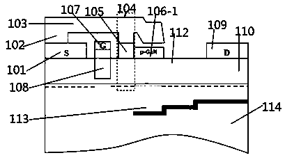
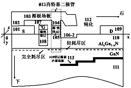
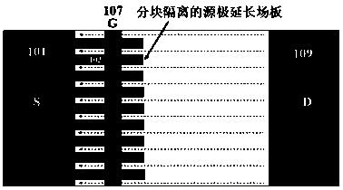
[0019] Such as figure 1 , figure 2 and image 3 As shown, a laterally diffused eGaN HEMT device integrating a reverse diode and an embedded drain field plate includes a GaN buffer layer 111, an AlGaN barrier layer 110, a gate electrode 107, an insulating layer under the gate 108, a source electrode 101, Source electrode extension 102, source field plate 103, MIS Schottky diode extension 104, MIS Schottky diode insulating layer 105, p-type GaN 106-1, groove 106-2, drain electrode 109, passivation Layer 112, AlN staggered drain embedded field plate 113; the GaN buffer layer 111 is grown on Si or sapphire or SiC substrate; the AlGaN barrier layer 110 is grown on the GaN buffer layer 111; the source The electrode 101 and the drain electrode are prepared on the surface of the AlGaN barrier layer 110, wherein the source electrode 101 is located ...
PUM
 Abstract
Description
Claims
Application Information