Low-doped tunneling field-effect transistor based on germanium-silicon heterojunction and double-gate technology and manufacturing method

A technology of tunneling field effect and manufacturing method, which is applied in the field of less-doped tunneling field effect transistors, can solve the problems of increasing the on-state current, etc., achieve the reduction of the tunneling distance, increase the on-state current, and improve the electron tunneling efficiency effect

Active Publication Date: 2020-09-08
XIDIAN UNIV
View PDF2 Cites 0 Cited by
  • Summary
  • Abstract
  • Description
  • Claims
  • Application Information

AI Technical Summary

Problems solved by technology

However, the tunneling efficiency of the electronic band of the low-doped tunneling field effect transistor DLTFET has not increased significantly, which limits the further improvement of the on-state current.

Method used


Image

  • Low-doped tunneling field-effect transistor based on germanium-silicon heterojunction and double-gate technology and manufacturing method
  • Low-doped tunneling field-effect transistor based on germanium-silicon heterojunction and double-gate technology and manufacturing method
  • Low-doped tunneling field-effect transistor based on germanium-silicon heterojunction and double-gate technology and manufacturing method

Examples


Embodiment Construction

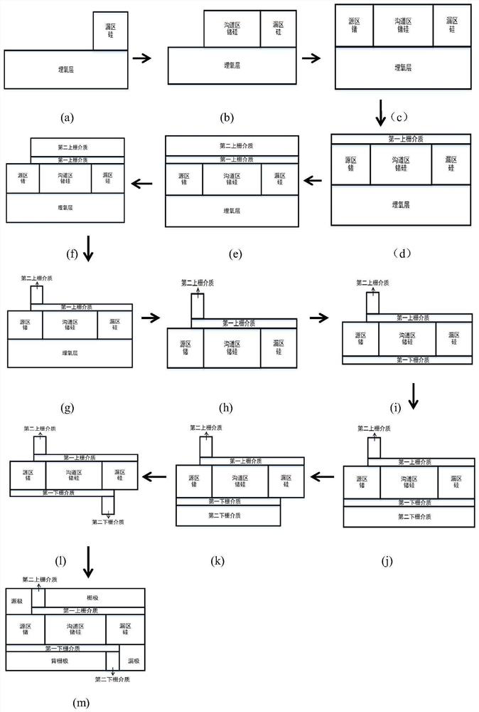
[0033] In order to make the objects and advantages of the present invention clearer, the present invention will be further described in detail below in conjunction with the accompanying drawings and embodiments.

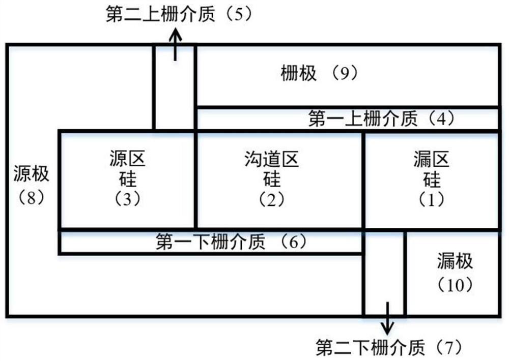
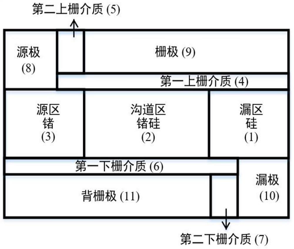
[0034] refer to figure 2 The device of the present invention includes a drain region 1, a channel region 2, a source region 3, a first upper gate dielectric 4, a second upper gate dielectric 5, a first lower gate dielectric 6, a second lower gate dielectric 7, and a source 8 , gate 9 and drain 10. in:

[0035] The channel region 2 has a height of 5±0.5nm, a length of 20±1nm, and a doping concentration of 1×10 18 / cm 3 , using germanium silicon material, which is located on the left side of the drain region 1, and is used to provide high channel carrier mobility;

[0036] The source region 3 has a height of 5±0.5nm, a length of 25±1nm, and a doping concentration of 1×10 18 / cm 3 , using a germanium material, which is located on the left side of the channel regi...


PUM

PropertyMeasurementUnit
heightaaaaaaaaaa
lengthaaaaaaaaaa
heightaaaaaaaaaa

Abstract

The invention discloses a less-doped tunneling field effect transistor based on a germanium-silicon heterojunction and double gates, and mainly solves the problems of poor switching ratio and frequency of an existing less-doped tunneling field effect transistor. The transistor comprises a drain region, a channel region, a source region, a first upper gate medium, a second upper gate medium, a first lower gate medium, a second lower gate medium, a source electrode, a grid electrode and a drain electrode, wherein the source region and the channel region are positioned on the left side of the drain region from left to right; the gate and the first upper gate medium are located on the upper side of the channel region from top to bottom, the first lower gate medium is located on the lower side of the channel region, the source is located on the left side of the first upper gate medium, the drain is located on the right side of the first lower gate medium, the second upper gate medium is located on the upper side of the first upper gate medium and the second lower gate medium; the source region and the channel region are respectively made of Ge and SiGe materials to form a heterojunction; and the back gate is positioned on the lower side of the first lower gate medium to form double gates. The switching ratio and frequency of the transistor are improved, and the transistor is suitable for a low-power-consumption digital integrated circuit.

Description

technical field [0001] The invention relates to the technical field of microelectronic devices, in particular to a less-doped tunneling field-effect transistor, which can be used in the preparation of large open-state current and low-power digital integrated circuits. Background technique [0002] In the field of low-power digital integrated circuits, with the improvement of device integration, the feature size of metal-oxide-semiconductor field-effect transistors based on traditional silicon is gradually reduced. When the size reaches the physical limit, metal-oxide-semiconductor field-effect transistors The manufacturing process becomes complicated, and it will also be affected by the short-channel hot carrier effect, channel carrier distribution quantum fluctuations, drain barrier reduction, negative bias temperature instability, and quantum tunneling effects, etc. Affected by various factors, the gate and channel of the metal oxide semiconductor field effect transistor w...

Claims


Application Information

Patent Timeline
Patent Type & Authority Patents(China)
IPC IPC(8): H01L29/165H01L29/739H01L21/331
CPCH01L29/165H01L29/66916H01L29/802
Inventor 刘红侠韩涛
Owner XIDIAN UNIV
Why Eureka
Try Eureka