GaAs HEMT (high electron mobility transistor) process-based positive-voltage-to-negative-voltage logic circuit

A logic circuit and negative pressure technology, applied in the direction of logic circuits using specific components, logic circuits, logic circuits using basic logic circuit components, etc., can solve system complexity and volume increase, cost increase, and increase system power consumption etc. to achieve high conversion efficiency, lower power consumption, and simple conversion structure

Pending Publication Date: 2019-09-17
NO 24 RES INST OF CETC
View PDF0 Cites 3 Cited by
  • Summary
  • Abstract
  • Description
  • Claims
  • Application Information

AI Technical Summary

Problems solved by technology

However, because the GaAs HEMT process is not compatible with the CMOS process, single-chip integration cannot be achieved, and only secondary integration is possible, resulting in increased system complexity, volume, and cost. At the same time, new devices also increase the power consumption of the system.

Method used


Image

  • GaAs HEMT (high electron mobility transistor) process-based positive-voltage-to-negative-voltage logic circuit
  • GaAs HEMT (high electron mobility transistor) process-based positive-voltage-to-negative-voltage logic circuit
  • GaAs HEMT (high electron mobility transistor) process-based positive-voltage-to-negative-voltage logic circuit

Examples


Embodiment 1

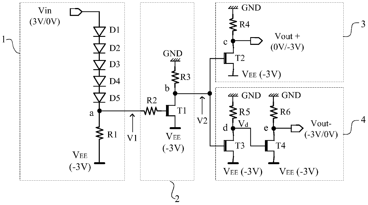
[0074] In detail, such as figure 2 As shown, the positive-to-negative-voltage logic circuit based on the GaAs HEMT process includes:

[0075] The input level shift circuit unit 1 performs level shift on the input positive voltage logic signal Vin to obtain the first negative voltage logic signal V1;

[0076] The buffer circuit unit 2 buffers and shapes the first negative logic signal V1 to obtain a second negative logic signal V2;

[0077] The non-inverting logic output circuit unit 3 adjusts the phase of the second negative logic signal V2 to obtain a third negative logic signal Vout+, and the third negative logic signal Vout+ is in phase with the positive logic signal Vin;

[0078] The inverting logic output circuit unit 4 adjusts the phase of the second negative logic signal V2 to obtain a fourth negative logic signal Vout-, and the fourth negative logic signal Vout- is inverted from the positive logic signal Vin;

[0079] Among them, the input level shift circuit unit 1...

Embodiment 2

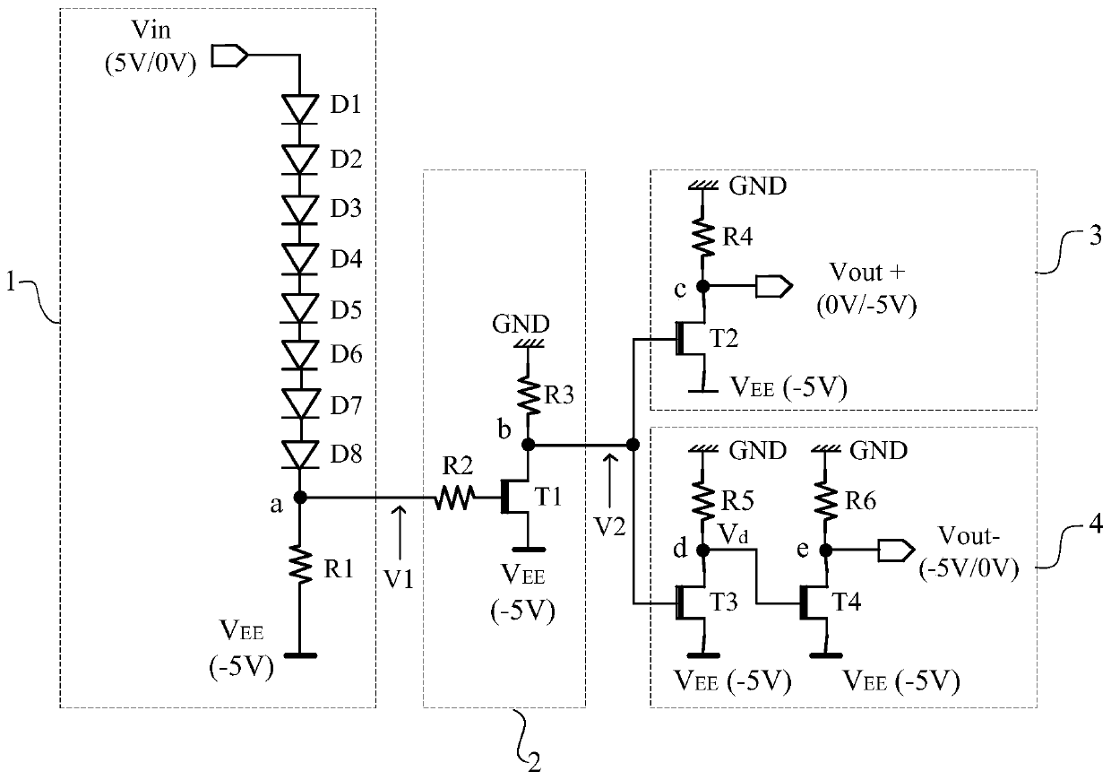
[0098] Embodiment 1 is aimed at the conversion of "3V / On, 0V / Off" positive voltage logic signal Vin (that is, its high level is 3V, and its low level is 0V), while for other specifications of positive voltage logic signal Vin The conversion is similar to the first embodiment. In the second embodiment of the present invention, the positive voltage logic signal Vin of "5V / On, 0V / Off" (that is, its high level is 5V, and its low level is 0V) is converted into "0V / On, -5V / Off" negative voltage logic signal (that is, its high level is 0V, and its low level is -5V).

[0099] In detail, such as image 3 As shown, the GaAs HEMT process-based positive voltage to negative voltage logic circuit in the embodiment of the present invention also includes:

[0100] The input level shift circuit unit 1 performs level shift on the input positive voltage logic signal Vin to obtain the first negative voltage logic signal V1;

[0101] The buffer circuit unit 2 buffers and shapes the first negativ...


PUM


Abstract

The invention provides a GaAs HEMT process-based positive voltage-to-negative voltage logic circuit. According to the positive-voltage-to-negative-voltage logic circuit, through the structural design of an input level shift circuit unit, a buffer circuit unit, an in-phase logic output circuit unit and a reverse-phase logic output circuit unit, an input positive pressure logic signal can be converted into two output complementary (in-phase and one-phase) negative pressure logic signals, the conversion structure is simple, and the conversion efficiency is high; each circuit unit is designed on the basis of a GaAs HEMT process, so that the positive-voltage-to-negative-voltage logic circuit can be directly integrated with a unit chip of a monolithic microwave integrated circuit such as a radio frequency switch, a numerical control attenuator and a numerical control phase shifter, the simplification and miniaturization of the application of the monolithic microwave integrated circuit system are promoted, and the power consumption of the monolithic microwave integrated circuit system is reduced.

Description

technical field [0001] The invention relates to the technical field of semiconductor integrated circuit design, in particular to a positive-voltage-to-negative-voltage logic circuit based on GaAs HEMT technology. Background technique [0002] In control-type single-chip microwave integrated circuits such as radio frequency switches, numerically controlled attenuators, and numerically controlled phase shifters, the control logic circuit is an indispensable unit circuit, which is used to realize digital logic such as switch on and off, attenuation / phase shift switching, etc. control function. Because GaAs-based HEMT transistors have significant characteristics such as high characteristic frequency, fast switching speed, good noise performance, and high output power, the current mainstream monolithic microwave integrated circuits use GaAs HEMT technology. [0003] Such as figure 1 As shown, the turn-on threshold of the enhancement-mode GaAs-based HEMT transistor is a positive...

Claims


Application Information

Patent Timeline
Patent Type & Authority Applications(China)
IPC IPC(8): H03K19/0175H03K19/173H03K17/567H03K17/74
CPCH03K17/567H03K17/74H03K19/017509H03K19/1733
Inventor 何峥嵘王国强刘成鹏蒲颜熊翼通潘少俊
Owner NO 24 RES INST OF CETC
Why Eureka
Try Eureka