A computational lithography modeling method and device

A computational lithography and modeling method technology, applied in the field of computational lithography modeling methods and devices, can solve the problems that the accuracy of optimization results cannot be guaranteed, the accuracy of computational lithography models cannot meet the lithography process, etc. The effect of precision

Active Publication Date: 2021-06-08
MOYAN COMPUTATIONAL SCI NANJING PTE LTD
View PDF4 Cites 0 Cited by
  • Summary
  • Abstract
  • Description
  • Claims
  • Application Information

AI Technical Summary

Problems solved by technology

In a set of computational lithography model parameters, the physical optics model parameters corresponding to an optical module, when simulating and fitting a test pattern, the fitting results obtained for different pattern units are different, which leads to When using the fitting results to optimize the model parameters, the accuracy of the optimization results cannot be guaranteed
Therefore, with the increasing complexity of the test pattern, the accuracy of the computational lithography model will not be able to meet the requirements of the lithography process

Method used


Image

  • A computational lithography modeling method and device
  • A computational lithography modeling method and device
  • A computational lithography modeling method and device

Examples


Embodiment Construction

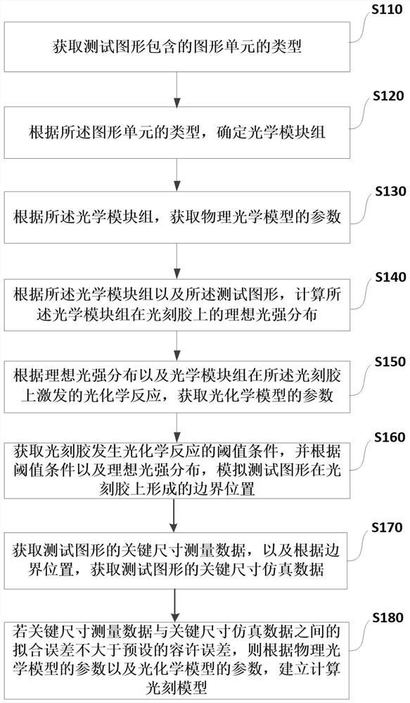
[0082] In order to improve the accuracy of the computational lithography model, the present application discloses a computational lithography modeling method and device through the following embodiments.

[0083] The first embodiment of the present application discloses a computational lithography modeling method, see figure 1 A schematic diagram of the workflow shown, the method includes:

[0084] Step S110: Obtain the type of graphic units included in the test pattern, where the test pattern refers to a reticle pattern used for testing.

[0085] Step S120: Determine an optical module group according to the type of the graphics unit, wherein the optical module group is composed of a plurality of optical modules.

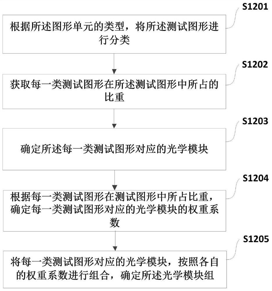
[0086] see figure 2 shown, figure 2 The schematic diagram of the workflow for determining the optical module group according to the type of the graphics unit disclosed in the embodiment of the present application includes:

[0087] Step S1201, classifying the ...


PUM


Abstract

This application relates to the technical field of integrated circuit manufacturing, and discloses a computational lithography modeling method and device. In this method, the optical module group is determined by obtaining the type of the graphic unit contained in the test pattern, and then according to the optical module group, the obtained Parameters of the physical optics model. Calculate the ideal light intensity distribution of the optical module group on the photoresist, and obtain the parameters of the photochemical model according to the ideal light intensity distribution and the photochemical reaction excited by the optical module group on the photoresist. Then simulate the boundary position of the test pattern formed on the photoresist, and obtain the critical dimension simulation data of the test pattern, if the fitting error between the critical dimension measurement data and the critical dimension simulation data is not greater than the preset allowable error, a computational lithography model is established. The computational lithography modeling method disclosed in the present application effectively improves the accuracy of the computational lithography model by establishing different optical modules to simulate different graphics units.

Description

technical field [0001] The present application relates to the technical field of integrated circuit manufacturing, and in particular, to a computational lithography modeling method and device. Background technique [0002] With the development of the lithography process, the size of the device in the integrated circuit manufacturing process has developed from sub-micron to ultra-deep sub-micron, that is, the key line width of the device is continuously reduced. With the shrinking of the key line width of the device, the Optical Proximity Effect (OPE) in the lithography process is becoming more and more prominent. OPE refers to the diffraction phenomenon and various physical and chemical effects of the lithography system. After the pattern on the reticle is transferred to the wafer surface, the obtained pattern produces various distortions, such as narrowing of the line width. In order to solve this problem, model-based Optical Proximity Correction (OPC) technology is usuall...

Claims


Application Information

Patent Timeline
Patent Type & Authority Patents(China)
IPC IPC(8): G03F7/20G06F30/20
CPCG03F7/705G06F30/39G06F30/20
Inventor 崔绍春
Owner MOYAN COMPUTATIONAL SCI NANJING PTE LTD
Why Eureka
Try Eureka