Supercharge Your Innovation With Domain-Expert AI Agents!

Image sensor and formation method thereof

An image sensor and pixel technology, which is applied in the manufacture of electrical solid-state devices, semiconductor devices, and semiconductor/solid-state devices, etc., can solve the problems of reduced device performance, large alignment deviation, and increased resistance, and achieve the effect of improving device performance.

Inactive Publication Date: 2019-09-20
HUAIAN IMAGING DEVICE MFGR CORP
View PDF2 Cites 0 Cited by
  • Summary
  • Abstract
  • Description
  • Claims
  • Application Information

AI Technical Summary

Problems solved by technology

[0005] However, in the existing Cu-Cu wafer bonding technology, the problem of large alignment deviation between corresponding pads is prone to occur, resulting in increased resistance and reduced device performance.

Method used


Image

  • Image sensor and formation method thereof
  • Image sensor and formation method thereof
  • Image sensor and formation method thereof

Examples


Embodiment Construction

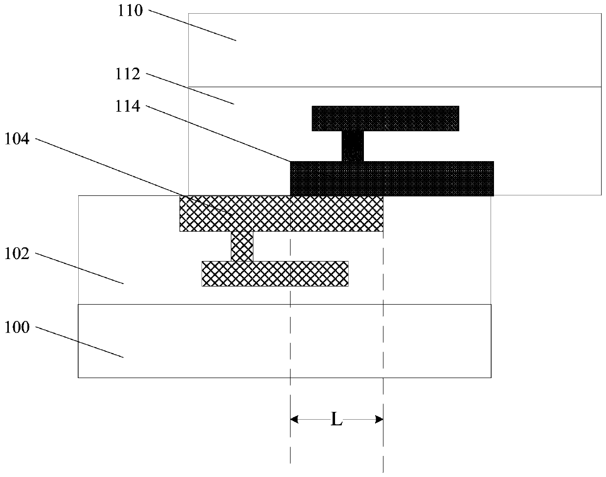
[0027] In the prior art, a logic wafer and a pixel wafer may be bonded by using metal bonding technology (such as Cu-Cu wafer bonding technology), so as to realize the interconnection function between the wafers. However, in the existing Cu-Cu wafer bonding technology, the problem of relatively large alignment deviation between corresponding pads is prone to occur, resulting in increased resistance and reduced device performance.

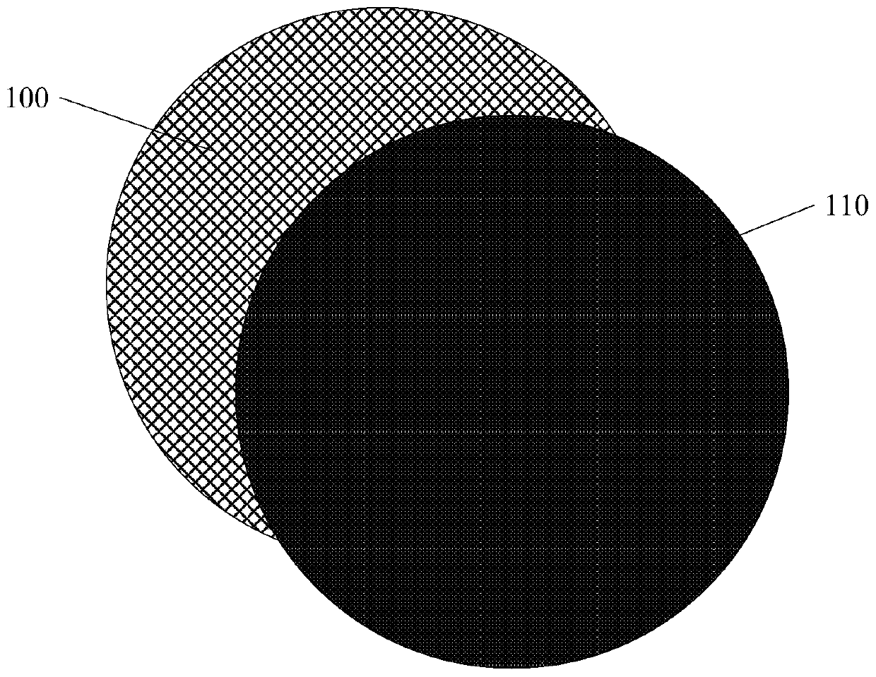
[0028] refer to figure 1 , figure 1 It is a schematic diagram of a working scene of wafer alignment in the prior art.

[0029] In a specific application, the first wafer 110 is usually grabbed by a robot arm, placed on the surface of the second wafer 100, and aligned, wherein the second wafer 100 can be fixed on the wafer substrate of the alignment chamber. seat.

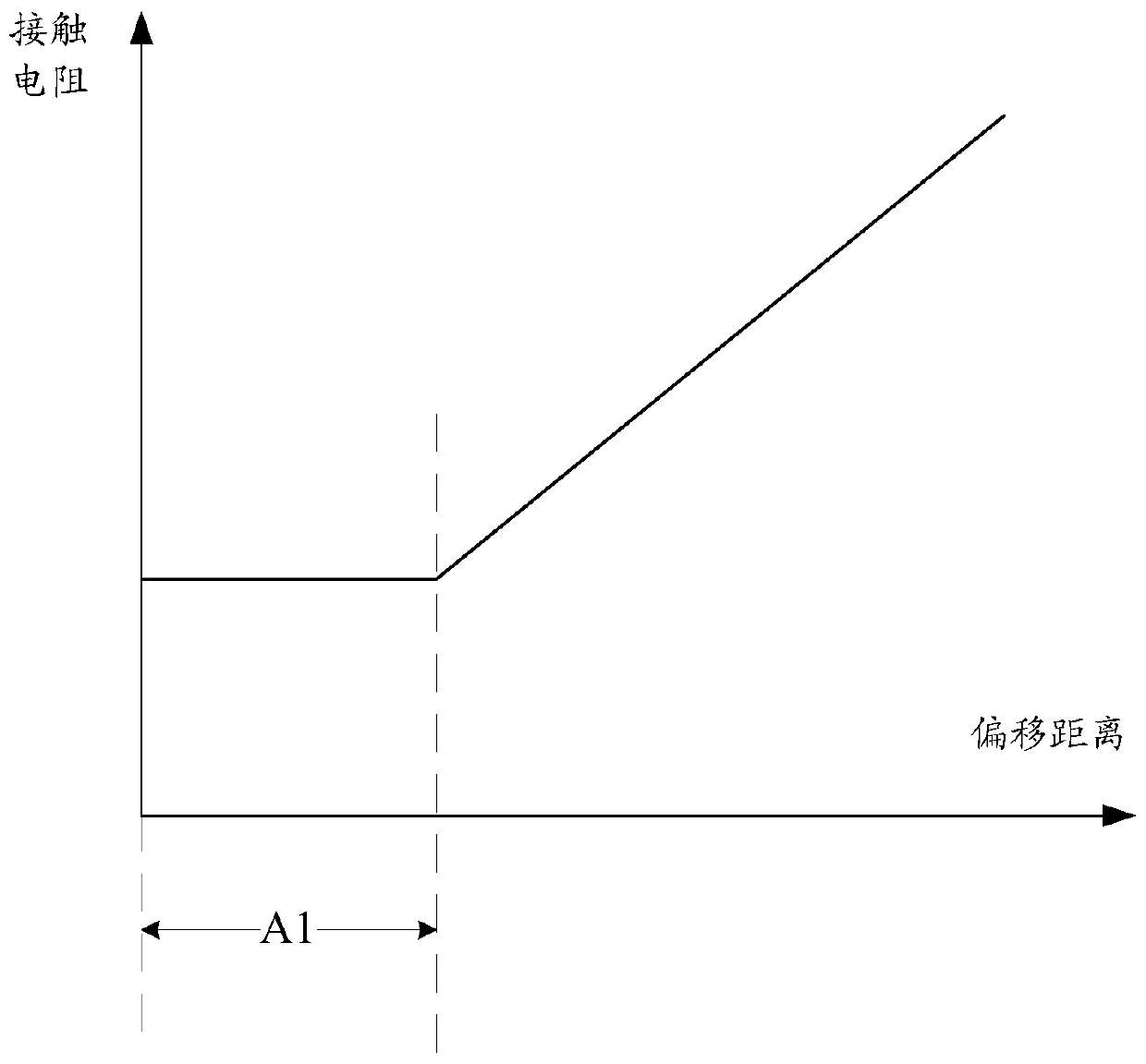
[0030] The inventors of the present invention have found through research that in the prior art, if the uniformity of the pad pattern is not good, it is easy to cause bonding problems ...


PUM


Abstract

The invention provides an image sensor and a formation method thereof. The method comprises the following steps: providing a first wafer, wherein the front surface of the first wafer has first liners; providing a second wafer, wherein the front surface of the second wafer has second liners, the second liners being in one-to-one correspondence with the first liners; and aligning the front surface of the first wafer to the front surface of the second wafer and carrying out bonding to make each first liner be electrically connected with the corresponding second liner, wherein the area of the surface of each first liner is smaller than the area of the surface of the corresponding second liner. The scheme can reduce the contact area of the first liners and the second liners, so that when there is a small degree of alignment deviation between the first wafer and the second wafer, the contact area is not affected, and alignment tolerance is broadened favorably.

Description

technical field [0001] The invention relates to the technical field of semiconductor manufacturing, in particular to an image sensor and a forming method thereof. Background technique [0002] The image sensor is the core component of the camera equipment, which realizes the image capture function by converting the optical signal into an electrical signal. Taking Complementary Metal Oxide Semiconductor Image Sensors (CMOS Image Sensors, CIS) devices as an example, due to their advantages of low power consumption and high signal-to-noise ratio, they have been widely used in various fields. [0003] 3D-Stack CIS was developed to support the demand for higher quality images. Specifically, 3D-Stack CIS can separately manufacture the logic wafer and the pixel wafer, and then bond the front side of the logic wafer and the front side of the pixel wafer, because the pixel part and the logic circuit part are independent of each other , so the pixel part can be optimized for high-qu...

Claims


Application Information

Patent Timeline
Patent Type & Authority Applications(China)
IPC IPC(8): H01L27/146H01L21/18
CPCH01L21/187H01L27/14601H01L27/14634H01L27/14683H01L27/14687
Inventor 周艮梅金子貴昭
Owner HUAIAN IMAGING DEVICE MFGR CORP
Features
  • R&D
  • Intellectual Property
  • Life Sciences
  • Materials
  • Tech Scout
  • Unparalleled Data Quality
  • Higher Quality Content
  • 60% Fewer Hallucinations
Learn More