Photoelectric device based on rhenium disulfide/tungsten diselenide heterojunction and preparation method

A technology of tungsten diselenide and rhenium disulfide, which is applied in the direction of electrical components, semiconductor devices, circuits, etc., can solve the problems of long response time, increased device cost, complex preparation process, etc., achieve fast response speed, low equipment requirements, The effect of simple process

Active Publication Date: 2019-09-24
HANGZHOU DIANZI UNIV
View PDF6 Cites 4 Cited by
  • Summary
  • Abstract
  • Description
  • Claims
  • Application Information

AI Technical Summary

Problems solved by technology

However, the deep bound states make ReS 2 Has a super long response time
In addition, currently based on ReS 2 PN optoel

Method used


Image

  • Photoelectric device based on rhenium disulfide/tungsten diselenide heterojunction and preparation method
  • Photoelectric device based on rhenium disulfide/tungsten diselenide heterojunction and preparation method
  • Photoelectric device based on rhenium disulfide/tungsten diselenide heterojunction and preparation method

Examples


example

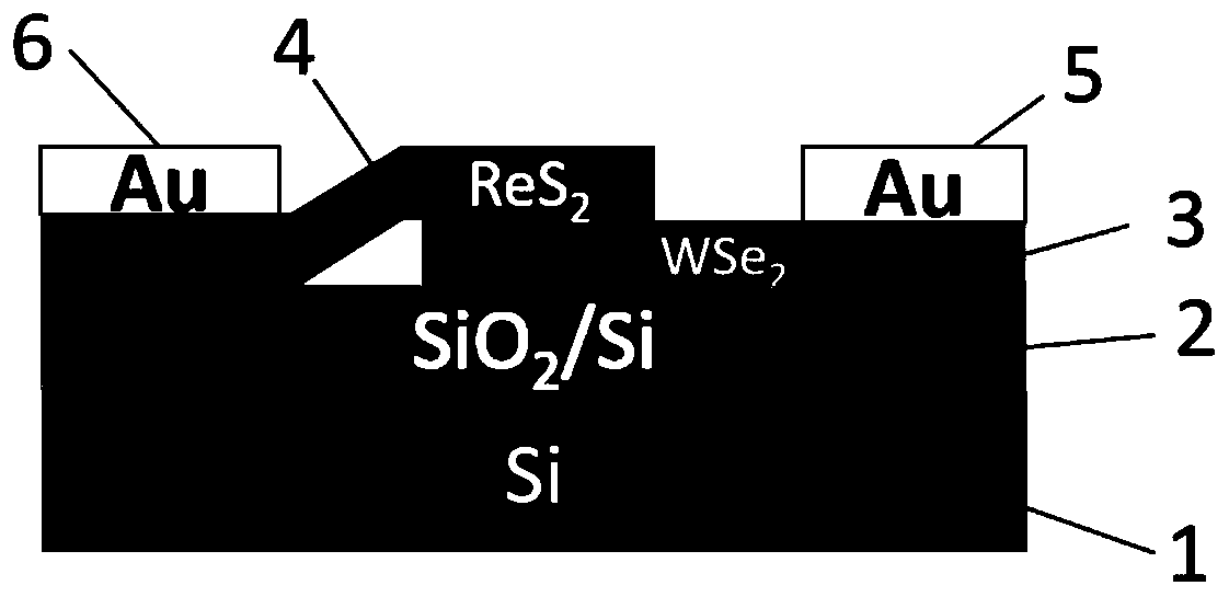
[0042] WSe in this implementation 2 Layer 3 is WSe 2 Single crystal layer, ReS 2 Layer is ReS 2 single crystal layer.

[0043] In the optoelectronic device prepared in this embodiment, the substrate is a Si substrate, and the insulating layer is SiO 2 The insulating layer and the electrode layer are Au electrodes. The resistivity of P-type Si substrate is less than 0.005Ω·cm, SiO 2 The thickness of the insulating layer is 300nm.

[0044] The specific preparation process is:

[0045] (1) Select a thermally oxidized silicon wafer as the substrate, firstly use ethanol, acetone, and deionized water to ultrasonicate for 5 minutes, then heat-treat the substrate on a heating platform at 300°C for 1 hour, and store it in a dry environment;

[0046] (2) Prepare scotch tape, and use a method similar to mechanical exfoliation of graphene to exfoliate a single layer of WSe on a silicon wafer 2 single crystal.

[0047] (3) Prepare PDMS (polydimethylsiloxane), cut PDMS into small s...


PUM

PropertyMeasurementUnit
Thicknessaaaaaaaaaa
Thicknessaaaaaaaaaa
Thicknessaaaaaaaaaa

Abstract

The invention discloses a photoelectric device based on a rhenium disulfide/tungsten diselenide (ReS2/WSe2) heterojunction and a preparation method, and belongs to the technical field of material application. The photoelectric device comprises a P-type silicon substrate, a silicon dioxide insulating layer, a heterojunction formed by single-layer ReS2 and WSe2, a drain electrode and a source electrode, wherein the source electrode, the drain electrode and the single-layer ReS2 and WSe2 are all located on a silicon dioxide/silicon (SiO2/Si) substrate, and Si is a grid electrode. The invention further discloses a simple method for preparing the photoelectric detection device. The photoelectric detection device realizes a wide barrier region and suppresses the influence of a defect state in ReS2 to the detector, thereby improving the response time of the detector.

Description

technical field [0001] The invention belongs to the field of optoelectronic functional devices, in particular to a photoelectric device based on a single-layer rhenium disulfide / tungsten diselenide heterojunction and a preparation method. Background technique [0002] Since the discovery of 2D graphene, a series of 2D materials with non-zero bandgaps, such as transition metal chalcogenides (TMDCs), black phosphorus (BP), and boron nitride (BN), have been continuously investigated, making up for the zero The shortcomings of graphene with a band gap in applications such as logic devices have promoted the development of two-dimensional materials in electronics and optoelectronics. TMDCs are considered to be promising electronic and optoelectronic materials due to their excellent low-dimensional stability, tunable band gap, strong photoluminescence, and optoelectronic devices with excellent performance in logic circuits. [0003] Defects are an integral part of the study of 2D ...

Claims


Application Information

Patent Timeline
IPC IPC(8): H01L31/0336H01L31/109H01L31/18
CPCH01L31/0336H01L31/109H01L31/1896Y02P70/50
Inventor 吴章婷洪锦涛张阳郑鹏郑梁
Owner HANGZHOU DIANZI UNIV
Why Eureka
Try Eureka