Band-pass filter based on tunable one-dimensional filter arrays and design method thereof
A band-pass filter and filter array technology, applied in waveguide-type devices, electrical components, circuits, etc., can solve the problems of low filter Q value, affect device performance, complicated design process, etc. Good frequency selectivity and stable tuning performance
- Summary
- Abstract
- Description
- Claims
- Application Information
AI Technical Summary
Problems solved by technology
Method used
Image

Examples
Embodiment 1
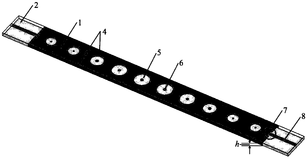
[0076] Example 1. like figure 1 and Figure 10 As shown, a single-layer one-dimensional filter array bandpass filter proposed by the present invention includes an upper metal layer 1, a dielectric substrate 2, a lower metal layer 3, and edge-wrapping metal layers 4 on both side walls of the dielectric substrate 2 , a circular EBG periodic unit 5 , an inner circular metal layer 6 , an input-output transition structure 7 , and a microstrip line 8 . Among them: circular ring (such as Figure 14 Shown) EBG periodic units 5 are etched on the upper metal layer 1, the number of EBG periodic units 5 is preferably not less than 3, generally 3 to 12, the EBG periodic units etched in Example 1 The number of 5 is 10; the microstrip line 8 is connected to the dielectric waveguide cavity through the input-output transition structure 7; the microstrip line 8 and the input-output transition structure 7 are based on the center line of the dielectric substrate 2 in the length direction and w...
Embodiment 2
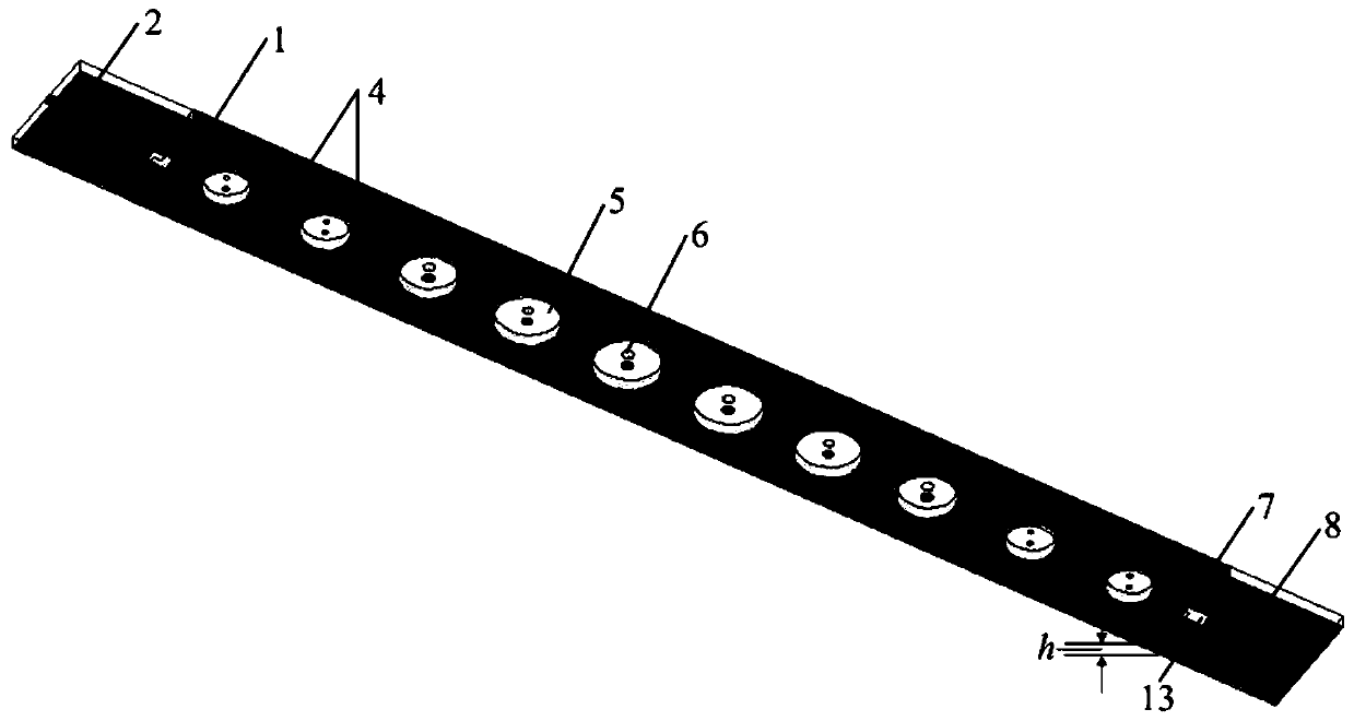
[0077] Example 2. like figure 2 As shown, a kind of double-deck one-dimensional filter array bandpass filter that the present invention proposes comprises upper metal layer 1, dielectric substrate 2, lower metal layer 3, the edge metal layer 4 of the two sidewalls of dielectric substrate 2, The shape of the medium is a circular EBG periodic unit 5 , an inner circular metal layer 6 , an input-output transition structure 7 , a microstrip line 8 , and a DGS structure 13 . figure 2 Directly below the microstrip line 8 and the input-output transition structure 7 , a rectangular DGS structure 13 is arranged on the center line of the wide side of the lower metal layer 3 . in:
[0078] ring (such as Figure 14 shown) EBG periodic units 5 are respectively etched on the upper metal layer 1 and the lower metal layer 3, the number of EBG periodic units on both the upper and lower metal layers is preferably not less than 3, generally 3 to 12 The number of EBG periodic units etched on...
Embodiment 3
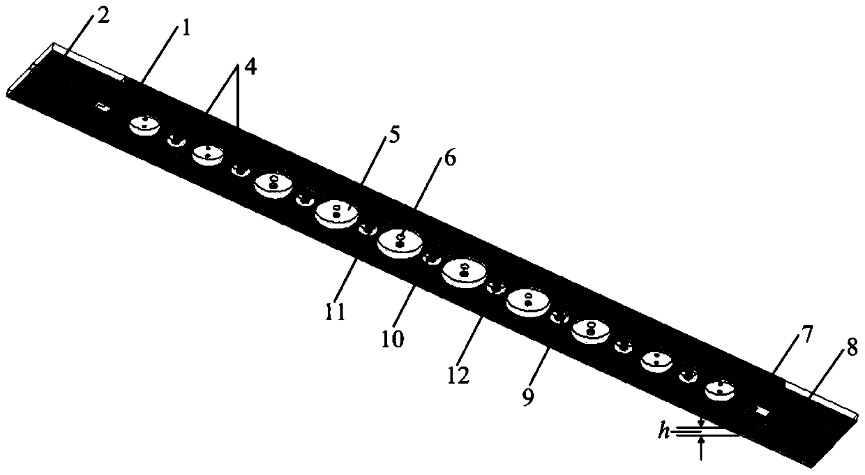
[0079] Example 3. like image 3 , Figure 4 , Figure 5 , Image 6 and Figure 11 As shown, a bandpass filter based on a tunable one-dimensional filter array proposed by the present invention includes an upper metal layer 1, a dielectric substrate 2, a lower metal layer 3, and edge-wrapped metal layers on both side walls of the dielectric substrate 2 4. The EBG periodic unit 5 with a medium shape of a ring, the inner metal layer 6, the input-output transition structure 7, the microstrip line 8, the anti-pad 9, the inner metal layer pad 10, and the varactor chip 11 , metal via 12 , DGS structure 13 . image 3 Directly below the microstrip line 8 and the input-output transition structure 7 , a rectangular DGS structure 13 is arranged on the center line of the wide side of the lower metal layer 3 . image 3 The shown tunable mechanism includes an anti-pad 9 , an inner circle metal layer pad 10 , a varactor diode chip 11 and a metal via 12 . in:
[0080] ring (such as Fi...
PUM
| Property | Measurement | Unit |
|---|---|---|
| Characteristic impedance | aaaaa | aaaaa |
| Thickness | aaaaa | aaaaa |
| Return loss | aaaaa | aaaaa |
Abstract
Description
Claims
Application Information
 - R&D
- Intellectual Property
- Life Sciences
- Materials
- Tech Scout
- Unparalleled Data Quality
- Higher Quality Content
- 60% Fewer Hallucinations
Browse by: Latest US Patents, China's latest patents, Technical Efficacy Thesaurus, Application Domain, Technology Topic, Popular Technical Reports.
© 2025 PatSnap. All rights reserved.Legal|Privacy policy|Modern Slavery Act Transparency Statement|Sitemap|About US| Contact US: help@patsnap.com