Graphene even harmonic frequency multiplier based on direct current bias and design method
An even-order harmonic and DC bias technology, which is applied in the field of graphene frequency multipliers, can solve the problem of low frequency multiplication efficiency of odd-order harmonic frequency multipliers, unstable performance of graphene frequency multiplier circuits, and inability to invest in a large scale Use and other problems to achieve good frequency multiplication effect and high frequency multiplication efficiency
- Summary
- Abstract
- Description
- Claims
- Application Information
AI Technical Summary
Problems solved by technology
Method used
Image
Examples
Embodiment 1
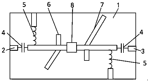
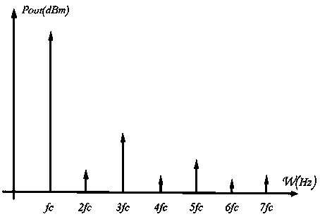
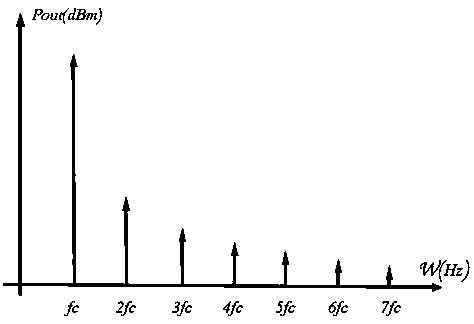
[0044] Embodiment 1: see Figure 1 to Figure 3 , a graphene even-order harmonic frequency multiplier based on DC bias, comprising a cavity, a signal input terminal 2, a signal output terminal 3, and a graphene frequency multiplier substrate in the cavity, the graphene frequency multiplier The substrate comprises a high-frequency dielectric substrate 1 and a graphene 8 arranged thereon, and the front end and rear end of the graphene 8 are respectively connected to the signal input terminal 2 and the signal output terminal 3 through a microstrip line, and is characterized in that:
[0045] On the microstrip line near the signal input terminal 2 and the signal output terminal 3, a first DC bias circuit and a second DC bias circuit are respectively provided, and the first DC bias circuit and the second DC bias circuit have the same structure , including a DC blocking capacitor 4 and a high-frequency inductor 5, the two ends of the DC blocking capacitor 4 are connected in series on...
Embodiment 2
[0062] Example 2: see Figure 1 to Figure 3 , a graphene even-order harmonic frequency multiplier based on DC bias, comprising a cavity, a signal input terminal 2, a signal output terminal 3, and a graphene frequency multiplier substrate in the cavity, the graphene frequency multiplier The substrate includes a high-frequency dielectric substrate 1 and a graphene 8 arranged thereon. The front end and rear end of the graphene 8 are respectively connected to the signal input terminal 2 and the signal output terminal 3 through a microstrip line, and the microstrip line is close to the signal input terminal. Terminal 2 and signal output terminal 3 are respectively provided with a first DC bias circuit and a second DC bias circuit, the first DC bias circuit and the second DC bias circuit have the same structure, including DC blocking capacitor 4 and High-frequency inductance 5, the two ends of the DC blocking capacitor 4 are connected in series on the microstrip line, one end of the...
Embodiment 3
[0082] Embodiment 3: according to the scheme of embodiment 2, we design a secondary frequency multiplier, that is to say, the frequency of the fundamental wave signal is fc, the frequency of the output signal is 2fc, and the signal frequency component nfc to be recovered, wherein n=1 , 2, 3, 4... and n≠2. All the other are identical with embodiment 2.
PUM
 Abstract
Description
Claims
Application Information


