

Solar cell and preparation method thereof
A solar cell and battery technology, applied in the field of solar cells, can solve the problems of low photoelectric conversion efficiency of solar cells, etc., and achieve the effects of compatible preparation process, improved light-receiving rate, and convenient industrial production.
- Summary
- Abstract
- Description
- Claims
- Application Information
AI Technical Summary
Problems solved by technology
Method used
Image

Examples
no. 1 example
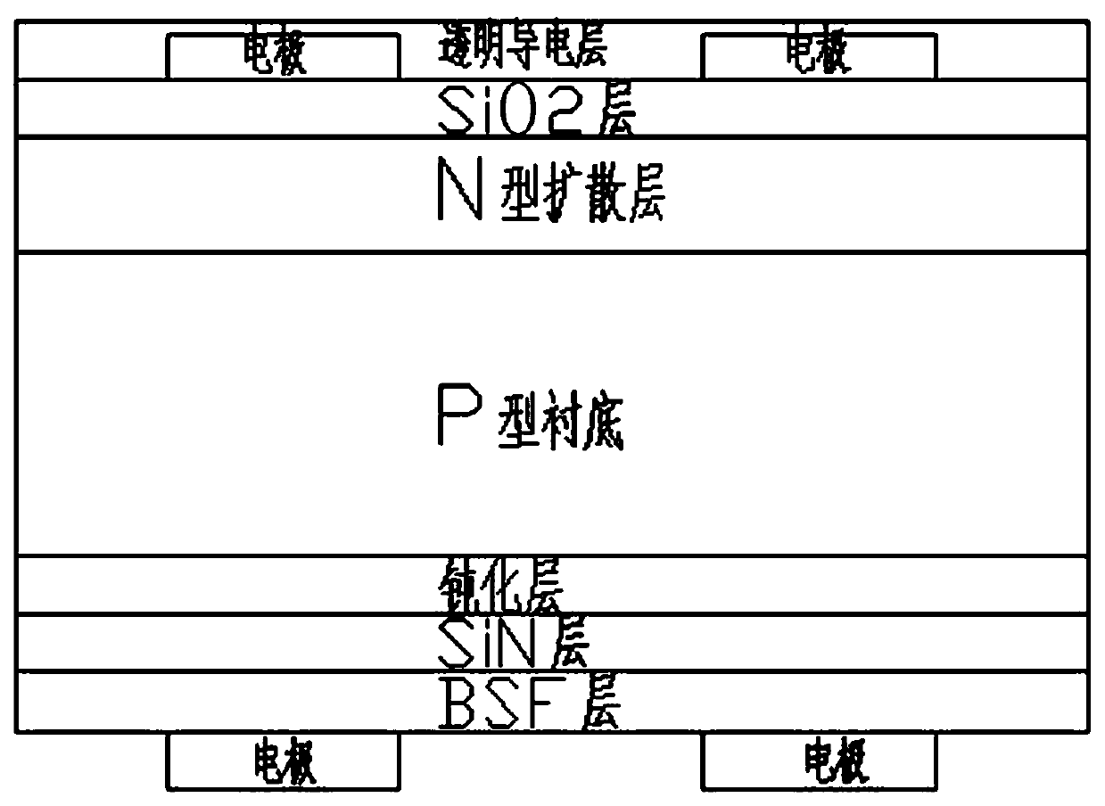
[0040] Such as Figure 1 to Figure 4 As shown, the structure of the single-polycrystalline P-type single-sided PERC cell of the present invention is given.
[0041] The specific preparation method is: provide a P-type single polycrystalline silicon wafer as a substrate (P-type substrate), the thickness of the selected P-type single polycrystalline silicon wafer is 150-300 microns, and on its surface (including the upper surface and the lower surface) ) for velvet treatment, the velvet grains of the velvet surface formed by velvet are 1-15 microns, and the reflectivity is 5-25%. Then perform phosphorous diffusion on the upper surface of the textured P-type single-polycrystalline silicon wafer to form an N-type diffusion layer. After the P-type single-polycrystalline silicon wafer is diffused with phosphorus, the sheet resistance is 50-140 ohms / □. Then perform wet etching on the P-type single polysilicon wafer after phosphorus diffusion. Wet etching will remove the phosphorus d...
no. 2 example
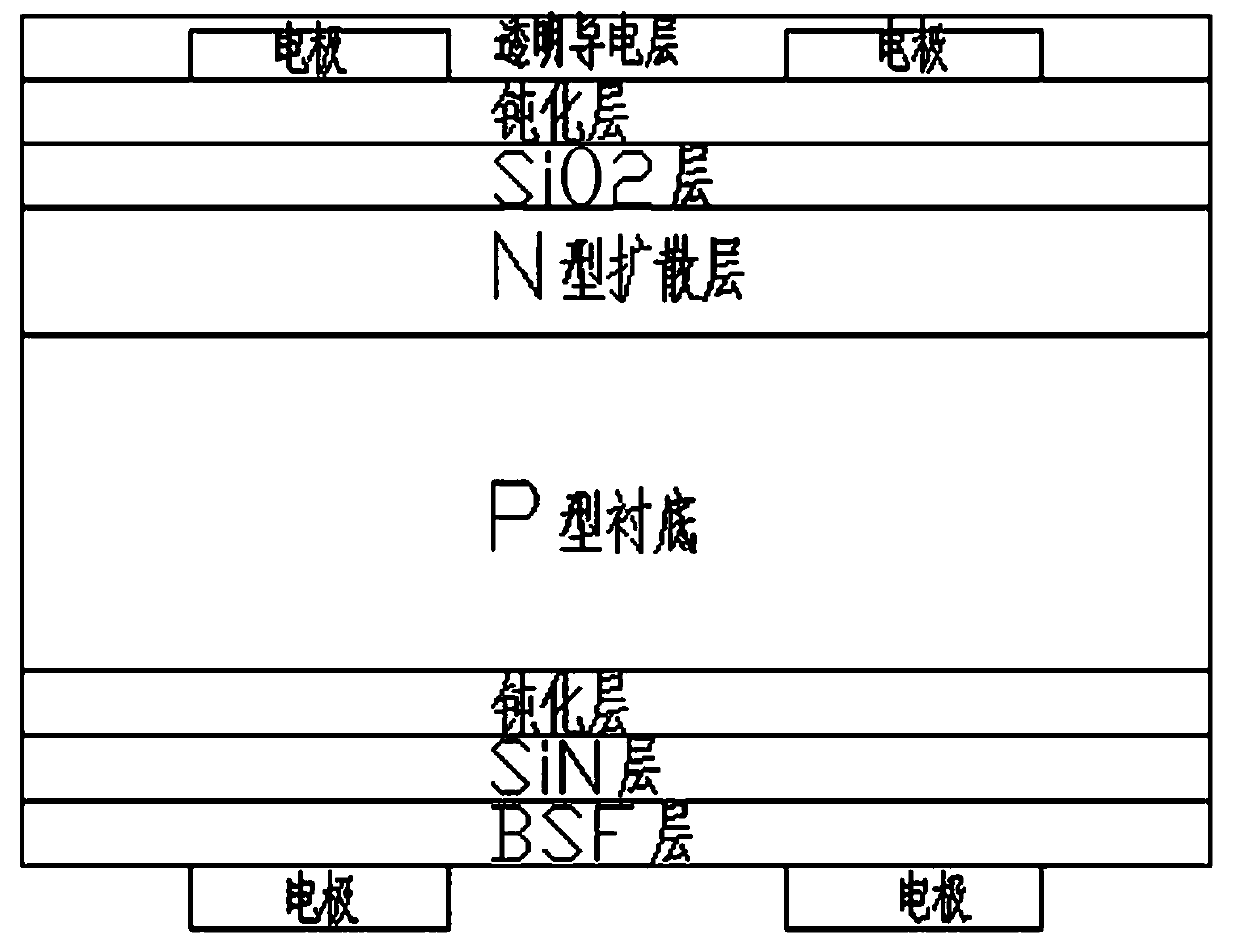
[0043] Such as Figure 5 to Figure 6 As shown, the structure of the single-polycrystalline P-type bifacial PERC cell of the present invention is given.
[0044] Its specific preparation method is: provide a P-type single-polycrystalline silicon wafer as a substrate, and perform texturing treatment on its surface. The thickness of the P-type single-polycrystalline silicon wafer is 150-300 microns, and the textured grains of the textured surface are 1 ~15 microns, with a reflectivity of 5~25%; Phosphorus diffusion is performed on the upper surface after texturing to form an N-type diffusion layer. Wet etching, wet etching will remove the phosphorus diffusion area on the lower surface (back side) and the phosphorosilicate glass part on the upper surface (front side); oxidation annealing is performed above the phosphorus diffusion surface to form an oxide layer (SiO 2 layer), the thickness of the oxide layer is about 1-10 nanometers; a passivation layer is grown on the oxide laye...
no. 3 example
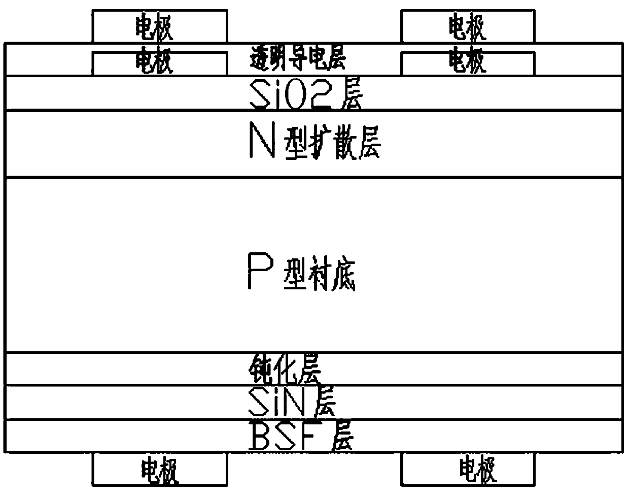
[0046] Such as Figure 7 to Figure 8 As shown, the structure of the single-polycrystalline N-type bifacial PERC cell of the present invention is given.
[0047] The specific preparation method is as follows: 1) Provide an N-type single-polycrystalline silicon wafer (N-type substrate), the thickness of the N-type single-polycrystalline silicon wafer is 150-300 microns, perform texturing treatment on the upper and lower surfaces, and form The velvet grains of the suede surface are 1-15 microns, and the reflectivity is 5-25%; 2) Then, boron is diffused on the upper surface after velvet making to form a P-type diffusion layer, and the square resistance of the silicon wafer after boron diffusion is 50-100 ohm / □; 3) Then perform wet etching on the boron-diffused N-type single polysilicon wafer. Wet etching will remove the boron diffusion area on the back and the borosilicate glass part on the front; The back of the wafer is heavily doped to form an N+ diffusion layer; 5) Then, the ...
PUM
| Property | Measurement | Unit |
|---|---|---|
| thickness | aaaaa | aaaaa |
| thickness | aaaaa | aaaaa |
| thickness | aaaaa | aaaaa |
Abstract
Description
Claims
Application Information