Mixed white light LED device with III-group nitride quantum well-metal-quantum dot mixed structure
A technology of LED devices and quantum dots, applied in semiconductor devices, electrical components, circuits, etc., can solve the problem of short coupling distance between quantum wells and quantum dots NRET, and achieve the effect of fast resonance energy transfer
- Summary
- Abstract
- Description
- Claims
- Application Information
AI Technical Summary
Problems solved by technology
Method used
Image
Examples
Embodiment 1
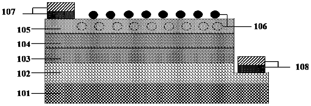
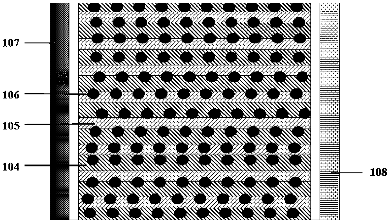
[0043] Such as Figure 1-2 As shown, the group III nitride quantum well-metal-quantum dot hybrid structure hybrid white LED device of this embodiment includes:
[0044] a sapphire substrate;
[0045] an n-type GaN layer grown on the substrate;
[0046] An In grown on the n-type GaN layer x Ga 1-x N / GaN quantum well active layer;
[0047] a p-type GaN layer grown on the quantum well active layer;
[0048] An ordered metal nano-grating array, the metal nano-grating array is arranged on the surface of the p-type GaN layer, and the gaps of the metal nano-grating array are filled with II-VI group quantum dots.
[0049] A p-type electrode fabricated on the metal nano-grating array;
[0050] An n-type electrode fabricated on the n-type GaN layer;
[0051] The thickness of the n-type GaN layer is 2um;
[0052] The quantum well active region x is 0.22, the emission wavelength is 465nm, the quantum well period is 10, and the thickness is 30nm;
[0053] The thickness of the p-ty...
Embodiment 2
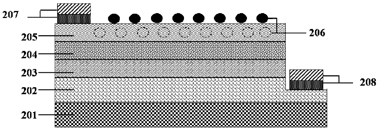
[0057] Such as Figure 3-4 As shown, the group III nitride quantum well-metal-quantum dot hybrid structure hybrid white LED device of this embodiment includes:
[0058] a sapphire substrate;
[0059] an n-type GaN layer grown on the substrate;
[0060] An In grown on the n-type GaN layer x Ga 1-x N / GaN quantum well active layer;
[0061] a p-type GaN layer grown on the quantum well active layer;
[0062] An ordered metal nanohole array, the metal nanohole array is arranged on the surface of the p-type GaN layer, and the gaps of the metal nano grating array are filled with II-VI group quantum dots.
[0063] A p-type electrode fabricated on the metal nanohole array;
[0064] An n-type electrode fabricated on the n-type GaN layer;
[0065] The thickness of the n-type GaN layer is 2um;
[0066] The quantum well active region x is 0.22, the emission wavelength is 465nm, the quantum well period is 10, and the thickness is 30nm;
[0067] The thickness of the p-type GaN layer...
Embodiment 3
[0071] Such as Figure 5-6 As shown, the group III nitride quantum well-metal-quantum dot hybrid structure hybrid white LED device of this embodiment includes:
[0072] a sapphire substrate;
[0073] an n-type GaN layer grown on the substrate;
[0074] An In grown on the n-type GaN layer x Ga 1-x N / GaN quantum well active layer;
[0075] a p-type GaN layer grown on the quantum well active layer;
[0076] annealing to form a disordered metal nano-layer, the metal nano-layer is arranged on the surface of the p-type GaN layer, and the gap of the metal nano-layer is filled with II-VI group quantum dots.
[0077] One ITO layer;
[0078] A p-type electrode is made on the ITO layer;
[0079] An n-type electrode fabricated on the n-type GaN layer;
[0080] The thickness of the n-type GaN layer is 2um;
[0081] The thickness of the ITO layer is 100nm;
[0082] The quantum well active region x is 0.22, the emission wavelength is 465nm, the quantum well period is 10, and the th...
PUM
| Property | Measurement | Unit |
|---|---|---|
| thickness | aaaaa | aaaaa |
| radius | aaaaa | aaaaa |
| thickness | aaaaa | aaaaa |
Abstract
Description
Claims
Application Information


