OLED for improving efficiency stability based on anode modification layer

An anode modification layer and stability technology, applied in the field of organic electroluminescent devices, can solve the problems of lowering the energy barrier of ITO and NPB, increasing the manufacturing cost and process difficulty, and unstable device efficiency, so as to improve the unstable efficiency and improve the efficiency of the device. Efficiency stability, good feasibility and reproducibility

Inactive Publication Date: 2019-10-29
CHONGQING UNIV OF POSTS & TELECOMM
View PDF2 Cites 1 Cited by
  • Summary
  • Abstract
  • Description
  • Claims
  • Application Information

AI Technical Summary

Problems solved by technology

[0004] Aiming at the problem of unstable device efficiency, the present invention designs an organic light-emitting diode that improves the stability of device efficiency. On the basis of the traditional OLED structure, MoO with different thicknesses is added to the anode 3 , using MoO 3 For the characteris

Method used


Image

  • OLED for improving efficiency stability based on anode modification layer
  • OLED for improving efficiency stability based on anode modification layer
  • OLED for improving efficiency stability based on anode modification layer

Examples


Example Embodiment

[0022] Example 1 (comparative example):

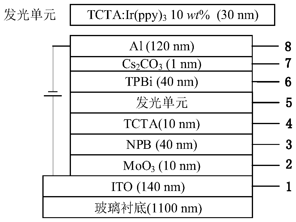
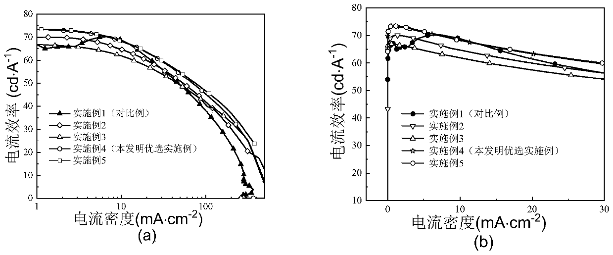
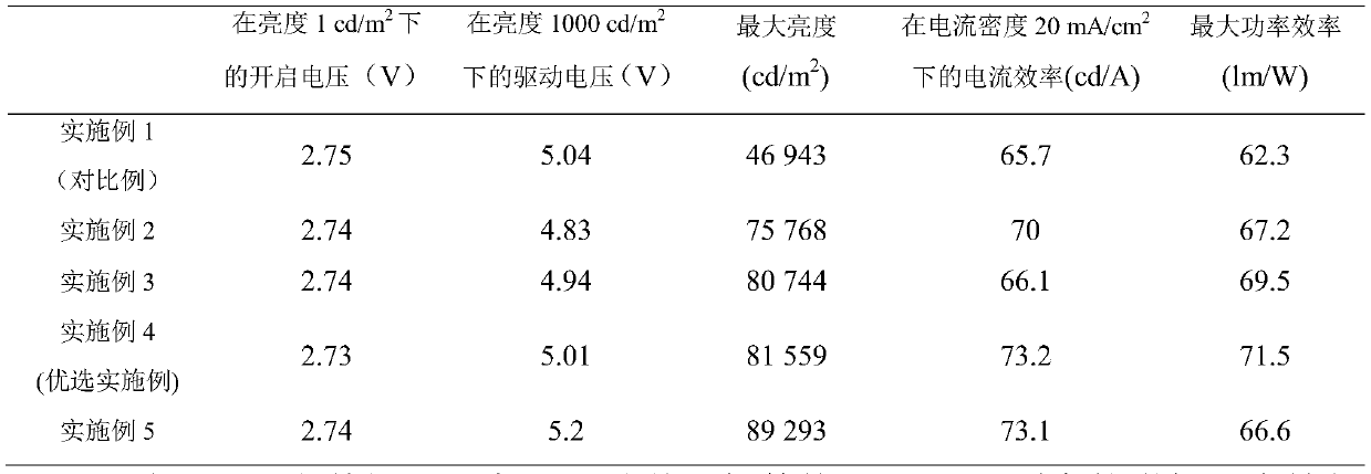
[0023] An organic electroluminescence device includes an anode, a hole injection layer, a hole transport layer, a light-emitting unit, an electron transport layer, an electron injection layer and a cathode arranged in sequence. The structure of the organic electroluminescent device of this embodiment is Glass (1100nm) / ITO (140nm) / NPB (40nm) / TCTA (10nm) / TCTA: Ir(ppy) 3 (10wt%,10nm) / TPBi(40nm) / Cs 2 CO 3 (1nm) / Al(120nm). The lighting voltage of the device in this embodiment is 2.75V, and the maximum brightness is 46943cd / m. 2 , The maximum power efficiency is 62.3lm / W, and the current density is 20mA / cm 2 The current efficiency is 65.7cd / A.

Example Embodiment

[0024] Example 2:

[0025] An organic electroluminescence device includes an anode, a hole injection layer, a hole transport layer, a light-emitting unit, an electron transport layer, an electron injection layer and a cathode arranged in sequence. The structure of the organic electroluminescent device of this embodiment is Glass (1100nm) / ITO (140nm) / MoO 3 (1nm) / NPB(40nm) / TCTA(10nm) / TCTA:Ir(ppy) 3 (10wt%,10nm) / TPBi(40nm) / Cs 2 CO 3 (1nm) / Al(120nm). The lighting voltage of the device in this embodiment is 2.74V, and the maximum brightness is 75 768cd / m. 2 , The maximum power efficiency is 67.2lm / W, and the current density is 20mA / cm 2 The current efficiency is 70cd / A.

Example Embodiment

[0026] Example 3:

[0027] An organic electroluminescence device includes an anode, a hole injection layer, a hole transport layer, a light-emitting unit, an electron transport layer, an electron injection layer and a cathode arranged in sequence. The structure of the organic electroluminescent device of this embodiment is Glass (1100nm) / ITO (140nm) / MoO 3 (5nm) / NPB(40nm) / TCTA(10nm) / TCTA:Ir(ppy) 3 (10wt%,10nm) / TPBi(40nm) / Cs 2 CO 3 (1nm) / Al(120nm). The lighting voltage of the device of this embodiment is 2.74V, and the maximum brightness is 80 744cd / m 2 , The maximum power efficiency is 69.5lm / W, and the current density is 20mA / cm 2 The current efficiency is 66.1cd / A.


PUM

PropertyMeasurementUnit
Thicknessaaaaaaaaaa
Thicknessaaaaaaaaaa
Brightnessaaaaaaaaaa

Abstract

The present invention claims an OLED (Organic Light Emitting Diode) for improving efficiency stability based on an anode modification layer. The OLED comprises a glass substrate, and an ITO anode, a buffer modification layer, a hole injection layer, a hole transport layer, a light-emitting layer, an electron transfer layer, an electron injection layer and a cathode are prepared on the glass substrate. The organic light emitting diode adopts MoO3 as the buffer modification layer, and the thickness of the MoO3 is 1nm, 5nm, 10nm and 20nm. Compared to a device without a modification layer, the problem of the unstable current efficiency of the device is obviously improved, and the brightness and the efficiency of the device are improved; and moreover, the preparation process of the device is simple, and the cost is low.

Description

technical field [0001] The invention belongs to the technical field of organic electroluminescent devices, in particular to an anode buffer modification layer for improving device efficiency and stability. Background technique [0002] Organic light-emitting diodes (Organic Light-Emitting Diode, OLED) have been widely concerned because of their huge application markets in the fields of flat panel display and solid-state lighting. Compared with other display technologies, OLED panels have many advantages, such as wide viewing angle, low driving voltage, fast response speed, flexible display, wide range of material selection, and full-color display in the 380nm-700nm spectral region. In line with the development trend of mobile communication and information display in the information age, as well as the requirements of green lighting technology, it has been developed and applied rapidly in the past 20 years. OLED uses organic small molecule materials as the materials of each ...

Claims


Application Information

Patent Timeline
IPC IPC(8): H01L51/50H01L51/52H01L51/54B82Y40/00
CPCB82Y40/00H10K50/17H10K50/814H10K2102/00
Inventor 王振谢嘉凤陈爱
Owner CHONGQING UNIV OF POSTS & TELECOMM
Why Eureka
Try Eureka