

Electromagnetic wave detector, electromagnetic wave detector array, and electromagnetic wave detection method
An electromagnetic wave and detector technology, which is applied in the field of electromagnetic wave detectors to achieve the effects of high sensitivity, high detection sensitivity and wide wavelength band
- Summary
- Abstract
- Description
- Claims
- Application Information
AI Technical Summary
Problems solved by technology
Method used
Image

Examples
Embodiment approach 1
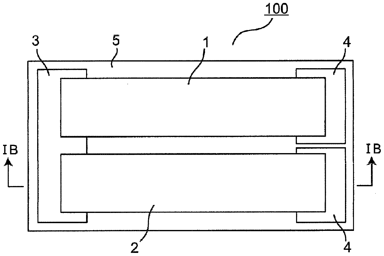
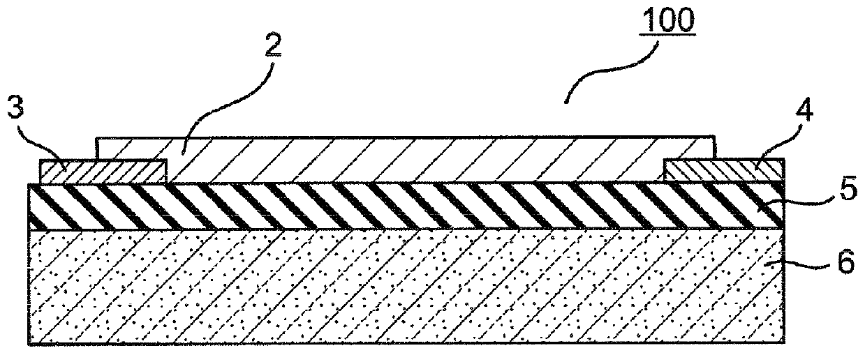
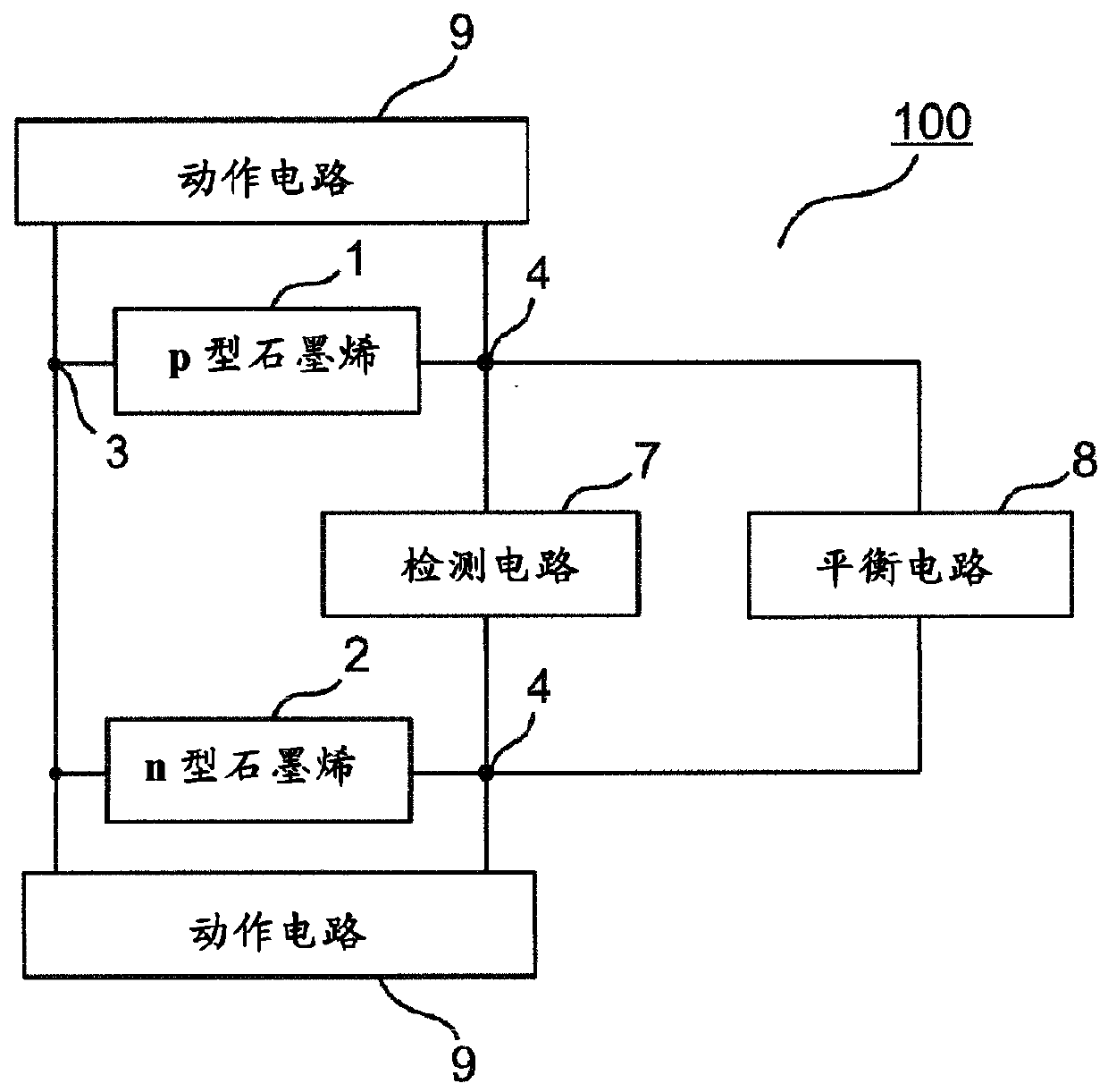
[0093] Figure 1A It is a plan view of the electromagnetic wave detector according to Embodiment 1 of the present invention, indicated by 100 as a whole, Figure 1B For viewing from 1B-1B direction Figure 1A A cross-sectional view of the case of the electromagnetic wave detector 100. in addition, Figure 1C It is a circuit diagram of the electromagnetic wave detector 100 according to Embodiment 1 of the present invention.
[0094] Such as Figure 1A , 1B As shown, the electromagnetic wave detector 100 includes a substrate 6 . The substrate 6 holds the entire electromagnetic wave detector 100 and is formed of a semiconductor material such as silicon. For example, a high-resistance silicon substrate or a substrate with improved insulation by forming a thermal oxide film is used. Alternatively, as will be described later, when using the substrate 6 as the back gate, a doped silicon substrate may also be used.
[0095] A layer comprising, for example, silicon oxide (SiO 2 ),...
Embodiment approach 2
[0126] Figure 3A It is a plan view of the electromagnetic wave detector according to Embodiment 2 of the present invention, indicated by 200 as a whole, Figure 3B For viewing from IIIB-IIIB direction Figure 3A A cross-sectional view of the case of the electromagnetic wave detector 200. exist Figure 3A , 3B in, with Figure 1A , 1B The same reference numerals indicate the same or corresponding parts.
[0127] In the electromagnetic wave detector 200 , an insulating layer 5 is formed on a substrate 6 , and a pair of electrodes 3 and 4 are provided on the insulating layer 5 . Graphene 11 is provided on insulating layer 5 so that both ends thereof are connected to electrodes 3 and 4 , respectively. In addition, a modulation circuit 15 for temporally varying the gate voltage is connected to the substrate 6 also serving as a gate electrode. In addition, a detection circuit 16 for detecting a differential photocurrent is connected between the electrodes 3 and 4 . The dete...
Embodiment approach 3
[0136] Figure 7A is a circuit diagram of an electromagnetic wave detector according to Embodiment 3 of the present invention, indicated by 300 as a whole, Figure 7B This is a circuit of the electromagnetic wave detector 300 according to Embodiment 3 of the present invention. exist Figure 7A , 7B in, with Figure 1C , 1D The same reference numerals indicate the same or corresponding parts.
[0137] The electromagnetic wave detector 300 of Embodiment 3 is different from the electromagnetic wave detector 100 of Embodiment 1 in that, as Figure 7A As shown, a differential amplifier circuit 10 is connected to the electrode 3 as a detection circuit. In the electromagnetic wave detector 100, it is necessary to use the balance circuit 8 to balance the circuit, but in the electromagnetic wave detector 300, since the differential current flowing through the p-type graphene 1 and the n-type graphene 2 in the bright state is used as The input of the differential amplifier circui...
PUM
 Abstract
Description
Claims
Application Information