Supercharge Your Innovation With Domain-Expert AI Agents!

Structure for improving quality of epitaxial layer of gallium nitride device and preparation method thereof

An epitaxial structure and gallium nitride technology, which is applied in the field of gallium nitride devices, can solve problems such as leakage reliability, epitaxial wafer warpage, thermal expansion coefficient mismatch, etc., to increase control ability, stabilize epitaxial structure, and balance internal stress Effect

Pending Publication Date: 2019-11-01
GLC SEMICON GRP CQ CO LTD
View PDF0 Cites 1 Cited by
  • Summary
  • Abstract
  • Description
  • Claims
  • Application Information

AI Technical Summary

Problems solved by technology

[0002] The technology of GaN epitaxy on the Si substrate in the internal structure of GaN devices, due to the mismatch of the lattice constant and the thermal expansion coefficient of GaN and the Si substrate, in order to avoid the remelting phenomenon of Ga atoms on the Si substrate, the Si substrate However, the lattice constant mismatch and thermal expansion coefficient mismatch between AlN and Si substrate, and the lattice constant mismatch and thermal expansion coefficient mismatch between GaN and AlN will cause GaN Poor quality of epitaxial layer and warpage of epitaxial wafer. Poor quality of epitaxial layer and high defect density will lead to decreased electron mobility, leakage and poor reliability of electronic devices. Warpage of epitaxial wafer will cause problems in the manufacturing process. Problems such as fragile chips and poor exposure yield of yellow light process
[0003] The current solution is to insert an AlGaN buffer layer with an appropriate Al content between GaN and AlN, because its lattice constant and thermal expansion coefficient are both between GaN and AlN, so as to obtain a buffer effect and slow down the effect caused by the lattice constant and thermal expansion coefficient. Disadvantages caused by excessive differences, but with the development of technology, the quality requirements of GaN channels are increasing and the development of large-scale epitaxial wafers, the existing technical solutions no longer meet the needs, and people are also conducting related research

Method used


Image

  • Structure for improving quality of epitaxial layer of gallium nitride device and preparation method thereof
  • Structure for improving quality of epitaxial layer of gallium nitride device and preparation method thereof
  • Structure for improving quality of epitaxial layer of gallium nitride device and preparation method thereof

Examples


Embodiment 1

[0029] A method and structure for improving the quality of an epitaxial layer of a gallium nitride device, the operation steps of which are as follows:

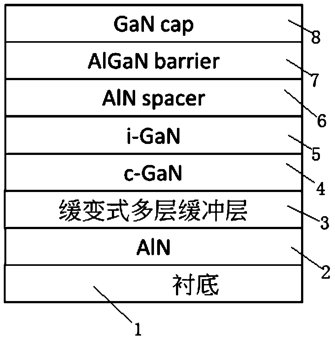
[0030] S1, growing an AlN buffer layer 2 on a planar or patterned Si or SiC substrate 1;

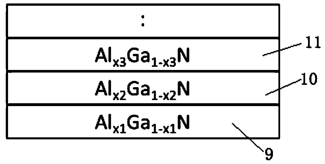
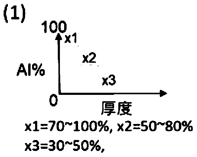
[0031] S2. After the growth of the AlN buffer layer 2 is completed, a slow-change multi-layer buffer layer 3 is grown above it, and the first layer is Al x1 Ga 1-x1 N buffer layer 9, where x1=1~0.7, namely Al 1~0.7 Ga 0~0.3 N, where x1 and 1-x1 represent their corresponding Al and Ga contents, Al x1 Ga 1-x1 The thickness of the N buffer layer 9 is 10-1000nm, which can be adjusted by adjusting Al x1 Ga 1-x1 The thickness of the N buffer layer 9 and the total number of layers of the slow-variable multi-layer buffer layer 3 are 3-10 layers to adjust the stress of the epitaxial structure. According to different epitaxial structure designs, different buffer layers are designed to reduce the difficulty of stress correction;

[0032] S3...

Embodiment 2

[0036] Embodiment 2: Based on Embodiment 1, the difference is:

[0037] A method and structure for improving the quality of an epitaxial layer of a gallium nitride device, the operation steps of which are as follows:

[0038] S1, growing an AlN buffer layer 2 on a planar or patterned Si or SiC substrate 1;

[0039] S2. After the growth of the AlN buffer layer 2 is completed, a slow-change multi-layer buffer layer 3 is grown above it, and the first layer is Al x1 Ga 1-x1 N buffer layer 9, where x1=1~0.7, namely Al 1~0.7 Ga 0~0.3 N, where x1 and 1-x1 represent their corresponding Al and Ga contents, respectively;

[0040] S3, in the first layer of Al x1 Ga 1-x1 After the growth of the N buffer layer 9 is completed, a second buffer layer structure is grown on it, and the second layer is Al x2 Ga 1-x2 N buffer layer 10, where x2=0.8~0.5, namely Al 0.8~0.5 Ga 0.2~0.5 N, where x2 and 1-x2 represent their corresponding Al and Ga contents, respectively;

[0041] S4, in the ...

Embodiment 3

[0053] Embodiment 3: Based on Embodiment 1 and 2, but the difference is:

[0054] Use a planar or patterned Si or SiC substrate 1 to insert a slowly variable multilayer buffer layer 3 between GaN and AlN. The slowly variable multilayer buffer layer 3 is formed by a multilayer AlGaN structure that grows sequentially. Due to the gradual change of the Al content Multi-layer structure, for the high defect density caused by lattice mismatch, it can more effectively solve the problem of lattice dislocation and improve the crystal quality of GaN channel layer more effectively, warpage caused by lattice stress, and thermal expansion mismatch The problem of internal stress accumulation is caused. Because the stress is uniformly processed by the AlGaN structure of each layer in multiple stages, it can be greatly improved, and a more stable epitaxial structure is also formed. The content of Al and Ga in AlGaN in the multilayer AlGaN structure changes slowly. Increase the ability to contr...


PUM

PropertyMeasurementUnit
thicknessaaaaaaaaaa
thicknessaaaaaaaaaa

Abstract

The invention discloses a structure for improving the quality of an epitaxial layer of a gallium nitride device and a preparation method thereof, and the problem of poor quality of an epitaxial layerof the existing gallium nitride device is solved. The structure comprises a substrate, an i-GaN layer and a GaN cap layer, the substrate is located at the lowest layer, the GaN cap layer is located atthe topmost layer, an AlN buffer layer is disposed on the upper portion of the substrate, a AlGaN barrier layer is disposed under the GaN cap layer. the i-GaN layer is disposed under the AlGaN barrier layer, a c-GaN layer is arranged at the lower portion of the i-GaN layer, a graded multilayer buffer layer is arranged between the c-GaN layer and the AlN buffer layer, and an AlN spacer layer is disposed between the AlGaN barrier layer and the i-GaN layer. The graded multilayer buffer layer is inserted between the GaN and the AlN by adopting the substrate, the graded multilayer buffer layer isformed by adopting the multi-layer AlGaN structure grown in order to greatly solve the warpage caused by lattice stress, and the internal stress accumulation due to thermal expansion mismatch and forma more stable epitaxial structure.

Description

technical field [0001] The invention relates to the field of gallium nitride devices, in particular to a structure for improving the quality of epitaxial layers of gallium nitride devices. Background technique [0002] The technology of GaN epitaxy on the Si substrate in the internal structure of GaN devices, due to the mismatch of the lattice constant and the thermal expansion coefficient of GaN and the Si substrate, in order to avoid the remelting phenomenon of Ga atoms on the Si substrate, the Si substrate However, the lattice constant mismatch and thermal expansion coefficient mismatch between AlN and Si substrate, and the lattice constant mismatch and thermal expansion coefficient mismatch between GaN and AlN will cause GaN Poor quality of epitaxial layer and warpage of epitaxial wafer. Poor quality of epitaxial layer and high defect density will lead to decreased electron mobility, leakage and poor reliability of electronic devices. Warpage of epitaxial wafer will caus...

Claims


Application Information

Patent Timeline
Patent Type & Authority Applications(China)
IPC IPC(8): H01L21/02
CPCH01L21/02381H01L21/02458H01L21/0254H01L21/02505
Inventor 廖宸梓王柏钧陈宪冠叶顺闵
Owner GLC SEMICON GRP CQ CO LTD
Features
  • R&D
  • Intellectual Property
  • Life Sciences
  • Materials
  • Tech Scout
  • Unparalleled Data Quality
  • Higher Quality Content
  • 60% Fewer Hallucinations
Learn More