

High-frequency low-noise amplifier circuit structure
A low-noise amplifier and circuit structure technology, applied in the field of amplifiers, can solve problems such as insufficient gain, large layout area, and low gain, and achieve stable DC working conditions, reduce manufacturing costs, and reduce layout area.
- Summary
- Abstract
- Description
- Claims
- Application Information
AI Technical Summary
Problems solved by technology
Method used
Image

Examples
Embodiment 1
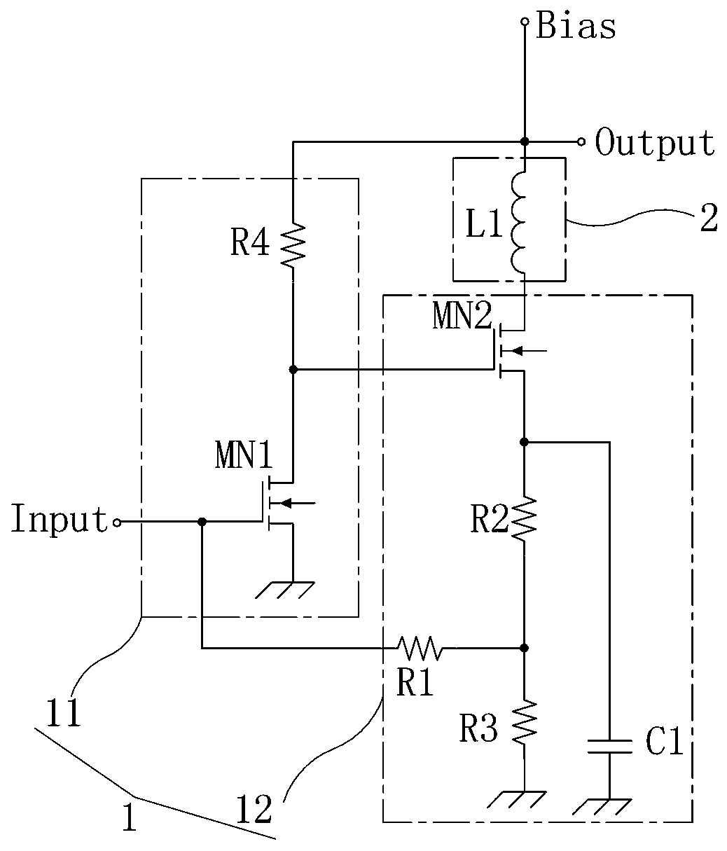
[0030] Such as image 3 As shown, in Embodiment 1 of the present invention, a high-frequency low-noise amplifier circuit structure includes a signal input terminal Input, a radio frequency amplifier circuit 1, a load 2, and a signal output terminal Output; wherein the radio frequency amplifier circuit 1 includes a stage A first-stage amplifying circuit 11 and a second-stage amplifying circuit 12 connected together; the first-stage amplifying circuit 11 is a single-ended amplifying circuit, and the first-stage amplifying circuit 11 includes a first field effect transistor MN1 and a fourth resistor R4; the second-stage amplifying circuit The circuit 12 is a single-ended amplifying circuit, and the secondary amplifying circuit 12 includes a second field effect transistor MN2, a first resistor R1, a second resistor R2, a third resistor R3 and a bypass capacitor C1; the load 2 is a load inductance L1 ; The gate of the first field effect transistor MN1 is connected to the signal inp...
Embodiment 2
[0034] Cooperate Figure 4As shown, the difference between the second embodiment of the present invention and the first embodiment is that: in the first embodiment, the second end of the fourth resistor R4 is directly connected to the first end of the load inductance L1 and the signal output end Output; and In the second embodiment, the second end of the fourth resistor R4 is connected to the first end of the load inductance L1 and the signal output terminal Output through the filter resistor R0 and the first filter capacitor C2, wherein the first end of the filter resistor R0 is connected to The first end of the load inductance L1 and the signal output end Output, the second end of the filter resistor R0 is connected to the first end of the first filter capacitor C2 and the second end of the fourth resistor R4, and the second end of the first filter capacitor C2 is grounded , the filter resistor R0 and the first filter capacitor C2 form an attenuation network to prevent the r...
Embodiment 3
[0036] Cooperate Figure 5 As shown, the difference between the third embodiment of the present invention and the second embodiment is that in the second embodiment, the first end of the first resistor R1 is directly connected to the gate of the first field effect transistor MN1 and the signal input terminal Input In the third embodiment, the first end of the first resistor R1 is connected to the gate of the first field effect transistor MN1 and the signal input terminal Input through a quarter filter FG and a second filter capacitor C3; The first end of the quarter filter FG is connected to the first end of the second filter capacitor C3 and the first end of the first resistor R1, the second end of the second filter capacitor C3 is grounded, and the quarter filter FG The second terminal is connected to the gate of the first field effect transistor MN1 and the signal input terminal Input; the quarter-wavelength filter FG, the third capacitor C3 and the first resistor R1 can fo...
PUM
 Abstract
Description
Claims
Application Information