Ceramic material laser processing device and method

A laser processing method and technology of ceramic materials, applied in laser welding equipment, metal processing equipment, manufacturing tools, etc., can solve the problems of large taper, easy edge collapse of hole wall, and small depth-to-diameter ratio, so as to disperse heat accumulation and improve laser utilization rate, reducing the effect of temperature gradient

Active Publication Date: 2019-11-05
BEIJING INST OF AEROSPACE CONTROL DEVICES
View PDF5 Cites 7 Cited by
  • Summary
  • Abstract
  • Description
  • Claims
  • Application Information

AI Technical Summary

Problems solved by technology

[0005] The technical problem solved by the present invention is: to overcome the deficiencies in the prior art, to propose a laser processing device and method for ceramic materials, for the laser drilling of ceramic materials, to overcome the current problems of small depth-to-diameter ratio, large taper, and easy hole walls of processed through holes. To solve problems such as chipping, the present invention provides a ceramic material laser processing device and me

Method used


Image

  • Ceramic material laser processing device and method
  • Ceramic material laser processing device and method

Examples


Embodiment Construction

[0043] The present invention will be further described in detail below in conjunction with the accompanying drawings and specific embodiments.

[0044] In order to make the object, technical solution and advantages of the present invention clearer, the present invention will be described in further detail below in conjunction with specific embodiments and with reference to the accompanying drawings. However, those skilled in the art know that the present invention is not limited to the drawings and the following embodiments.

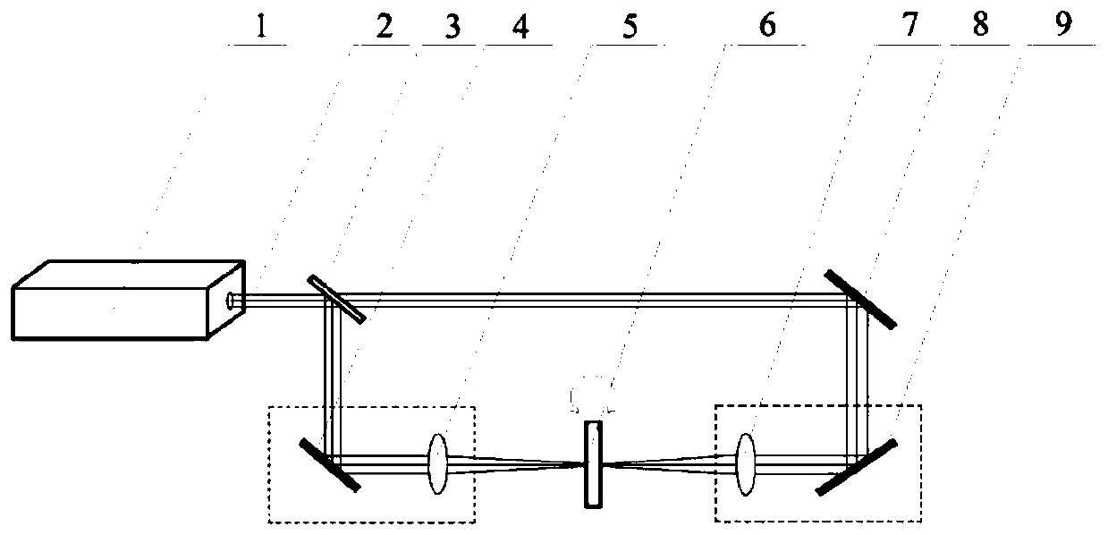
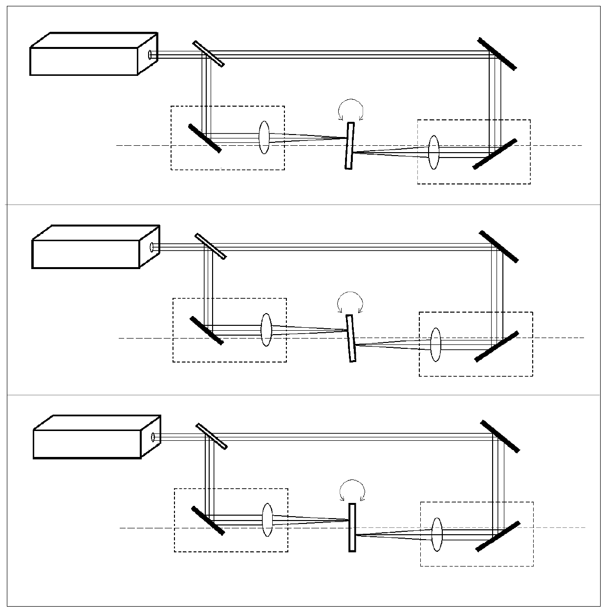
[0045]A ceramic material laser processing device and method of the present invention, for laser drilling of ceramic materials, solves the existing problems of small depth-to-diameter ratio, large taper, and easy edge collapse of the hole wall, etc., and realizes high-quality drilling of ceramic materials. To meet the needs of ultra-high frequency communication electronics industry for micro-processing of ceramic packaging substrates. The depth-to-diamet...


PUM


Abstract

The invention discloses a ceramic material laser processing device and method. According to the ceramic material laser processing device and method, for laser perforating of a ceramic material, the problems that in the prior art, the depth-diameter ratio of a machined through hole is small, the taper is large, the hole wall is prone to breakage are solved, high-quality perforating of the ceramic material is realized, the requirement for micro processing on a ceramic packaging substrate of the ultrahigh-frequency communication electronic industry is met, the processing dip angle of laser perforating is synchronously and orderly regulated and controlled through sequential operation of clockwise rotation, anticlockwise rotation and adjustment of a ceramic chip, and then the hole wall taper iseffectively reduced. Meanwhile, the double-sided processing mode effectively disperses heat accumulation, reduces the temperature gradient, reduces the damage of heat influence on the ceramic material, and reduces the edge breakage of the hole wall. Particularly, under the mode of performing focusing by adopting a cone lens, a bessel space distribution light beam is obtained, namely, a transverselight spot (the transverse direction is the perpendicular light beam propagation direction) after the laser beam is focused is reduced, a longitudinal light spot (the longitudinal direction is the parallel light beam propagation direction) after the laser beam is focused is stretched, the laser utilization rate is effectively improved, and the heat influence is reduced.

Description

technical field [0001] The invention relates to a ceramic material laser processing device and method, in particular to a laser processing device and method capable of realizing high-quality drilling of ceramic materials, and belongs to the technical field of ceramic laser processing. Background technique [0002] With the rapid development of the communication electronics industry, traditional plastic and metal substrates have been difficult to meet the requirements of UHF. Ceramic materials have outstanding electrical insulation properties, excellent high-frequency characteristics, good matching of electronic components, and stable Advantages such as chemical properties are more and more widely used in the field of packaging substrates. [0003] Ceramic materials are typical hard and brittle materials, which are difficult to process due to their high hardness and high brittleness. Traditional ceramic processing mainly uses mechanical methods such as turning, cutting, etch...

Claims


Application Information

Patent Timeline
IPC IPC(8): B23K26/382B23K26/70B23K26/04
CPCB23K26/04B23K26/382B23K26/70B23K26/702
Inventor 高文焱王军龙李本海李广雷名威李凯张路侯振兴
Owner BEIJING INST OF AEROSPACE CONTROL DEVICES
Why Eureka
Try Eureka