Novel terahertz temperature-controlled adjustable multi-frequency metamaterial absorber

A terahertz and metamaterial technology, applied in the field of new terahertz temperature-controlled multi-frequency metamaterial absorbers, can solve the problems of complex and different metamaterial absorbers, and achieve stable physical properties and not easy to damage. Effect

Inactive Publication Date: 2019-11-12
ZHONGBEI UNIV
1 Cites 3 Cited by

AI-Extracted Technical Summary

Problems solved by technology

The preparation of traditional electromagnetic absorbing coating materi...

Abstract

The invention relates to design and preparation of a novel terahertz temperature-controlled adjustable multi-frequency metamaterial absorber. The design idea includes the following steps: according tothe current development status of a temperature-control material, InSb is selected as a metamaterial absorber dielectric substrate, and according to a Drude model, the relative dielectric constant issubjected to approximate calculation and extraction; based on the traditional sandwich absorbing structure design principle, a finite-difference time-domain method is used for modeling and simulationto design a metamaterial metal unit formed by combing polarization-insensitive L-shaped four corners and a middle built-in zigzag structure, and finally, a magnetron sputtering process and a metal stripping process are carried out for sample preparation. The multi-frequency temperature-controlled metamaterial unit design and process preparation is the core technology, and in comparison with the traditional absorbing material, more absorbing frequency bands are achieved, the flexibility is better, and the manufacturing accuracy is higher.

Application Domain

Technology Topic

Image

  • Novel terahertz temperature-controlled adjustable multi-frequency metamaterial absorber
  • Novel terahertz temperature-controlled adjustable multi-frequency metamaterial absorber
  • Novel terahertz temperature-controlled adjustable multi-frequency metamaterial absorber

Examples

  • Experimental program(1)

Example Embodiment

[0025] A new type of terahertz temperature-controlled adjustable metamaterial absorber, the design idea includes the following steps:
[0026] Combined with the traditional "sandwich" wave absorbing structure, the original dielectric layer is replaced with temperature-controlled InSb material, and then the bottom of the metal plate is sputtered, and the metal unit structure is prepared on the upper surface. The specific process is as follows : First, the InSb film is prepared by the three-temperature zone method, and then the bottom metal plate is prepared by magnetron sputtering, and the MEMS metal peeling process is used for the preparation of the metal unit.
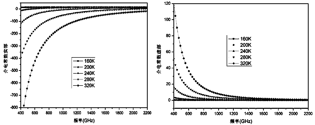
[0027] InSb thin film is a semiconductor thin film with high electron mobility. Here, vacuum coating technology is used to prepare InSb thin films on silicon wafers. In the preparation process, inert gases such as nitrogen and helium are used for protection, and the three-temperature zone method is used to control the temperature of the two evaporation sources and the silicon substrate, so that the concentration of Sb molecules after film formation is low, that is, in an In-rich state. In the second half of the heat treatment process, due to the degradation of the eutectic point, the In solid phase will be precipitated, so the InSb-In eutectic is obtained, and then the InSb crystal is precipitated by the heat treatment method. After the InSb crystal is obtained, the metamaterial metal base plate is made by magnetron sputtering technology, and then the combination of the InSb crystal and the InSb crystal are peeled off from the silicon wafer, so that the InSb is on the upper side, and then parylene deposition is performed on the surface to improve the unit metal Adhesiveness, and then process processes such as homogenization, photolithography, development, magnetron sputtering, and metal stripping on the surface.
[0028] The preparation process of the metal unit using the MEMS metal peeling process is as follows: first, the glue is homogenized on InSb, and the glue used is AZ5214E. Drop the glue on the InSb, then place it on the homogenizer, the low speed is 600r/min, and the acceleration is set to 600m/s 2 , Spreading time is 6s, then high speed 4000r/min, acceleration is 2000m/s 2 , The homogenization time is 30s, which will form a colloidal film. Next, pre-bake the film glue after homogenization, the temperature is 95℃, the drying time is 90s, then it is cooled to room temperature, and then the mask is exposed; after the exposure, the reverse baking is performed immediately, the temperature is 105℃, and the drying The time is 2 minutes, and then pan exposure is performed after cooling to room temperature. After the exposure is completed, use 238 developer to develop the glue. The development time is about 40s. Rinse with a small dose of deionized water for about 50s, and then use a small dose of nitrogen to dry it. The dried object is placed in a sputtering machine, and 1 micron thick copper is sputtered. The sputtered product is finally peeled off, and the object is placed in an acetone solution. The reason is that the AZ5214E ​​colloid is dissolved in acetone, which facilitates the separation of the metal on the colloid from the metal on the dielectric substrate, and then leaves the metal structure on the dielectric substrate . Finally, rinse the stripped product with deionized water, dry it with nitrogen and cover it with glassware for use.
[0029] The present invention designs the size of the metamaterial unit according to the current terahertz radar band, and analyzes the performance of the temperature control material indium antimonide (InSb) through the finite difference time domain method modeling simulation analysis. The dielectric constant and permeability in the frequency band of ~2200GHz are extracted and the parameters are analyzed; in the temperature range of 160-320K, the relative dielectric constant of InSb can be approximated by a simple Drude model:
[0030]
[0031] ε ∞ It represents the high-frequency dielectric constant angular frequency, the angular frequency of InSb is usually selected as 15.6, γ is the damping constant, and the plasma frequency Depends on the intrinsic carrier density N, the electron charge is e, and the vacuum dielectric constant is ε 0 , The effective mass of free carriers is m *. The intrinsic carrier density N of metallic copper can be calculated by consulting related literature.

PUM

no PUM

Description & Claims & Application Information

We can also present the details of the Description, Claims and Application information to help users get a comprehensive understanding of the technical details of the patent, such as background art, summary of invention, brief description of drawings, description of embodiments, and other original content. On the other hand, users can also determine the specific scope of protection of the technology through the list of claims; as well as understand the changes in the life cycle of the technology with the presentation of the patent timeline. Login to view more.

Similar technology patents

Positive rhythm reservoir combined polymer type profile control agent and using method thereof

InactiveCN107236526ASealed firmlyStable physical propertiesCleaning apparatusDrilling compositionWater cycleBlocking layer
Owner:DALIAN DONGYOU RUIJIA PETROLEUM TECH CO LTD

Anti-reflective glass with ultra-large panel and preparation method thereof

InactiveCN107640910AStable physical propertiesSolve the requestTemperature resistanceSilicon nitride
Owner:SHANGHAI NORTHGLASS COATING TECH IND

Classification and recommendation of technical efficacy words

  • Not easy to damage
  • Stable physical properties

Selectively hydrogenating catalyst and preparation method thereof

ActiveCN101433845AStable physical propertiesActiveMetal/metal-oxides/metal-hydroxide catalystsRefining by selective hydrogenationPalladiumMetal
Owner:PETROCHINA CO LTD

Preparation for PRRSV-N-IgY antibody and application thereof in detecting PRRSV

InactiveCN101717446AStable physical propertiesReduce the rate of false positivesEgg immunoglobulinsImmunoglobulins against virusesAntigenGlobulin
Owner:ZHEJIANG UNIV

Gas metastable atom beam generation device adopting fluid cooling

InactiveCN106068054AStable temperatureStable physical propertiesMasersAcceleratorsEngineeringPre cooling
Owner:PLA PEOPLES LIBERATION ARMY OF CHINA STRATEGIC SUPPORT FORCE AEROSPACE ENG UNIV

High-performance capacitor film

InactiveCN104140592AStable physical propertiesGood mechanical strengthPolypropylenePOLYETHYLENE WAX
Owner:宁国市裕华电器有限公司
Why Eureka
Try Eureka