UV LED chip of P-type GaN layer and preparation method thereof

A chip, p-type technology, applied in the field of optoelectronics, can solve problems such as the absorption of ultraviolet outgoing light that cannot be well avoided, and achieve the effect of improving external quantum efficiency and luminous power and reducing absorption.

Inactive Publication Date: 2019-11-15
SHANDONG INSPUR HUAGUANG OPTOELECTRONICS
View PDF24 Cites 3 Cited by
  • Summary
  • Abstract
  • Description
  • Claims
  • Application Information

AI Technical Summary

Problems solved by technology

However, for shorter wavelengths of ultraviolet light, the technology describe

Method used


Image

  • UV LED chip of P-type GaN layer and preparation method thereof
  • UV LED chip of P-type GaN layer and preparation method thereof

Examples


Embodiment 1

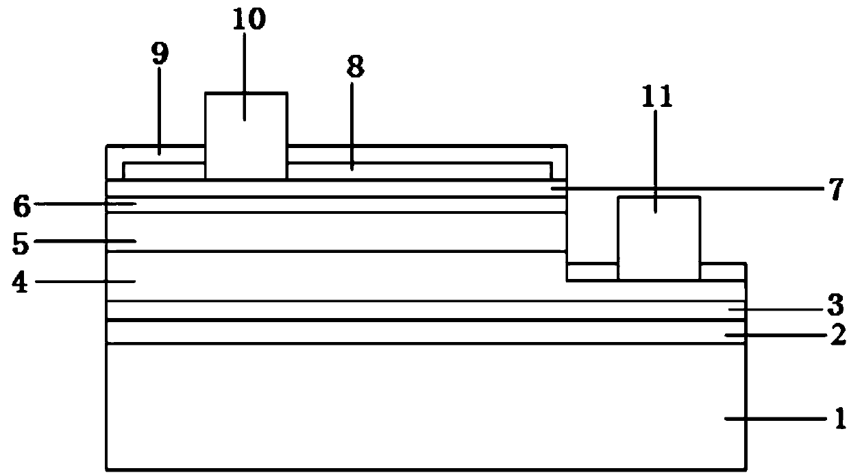
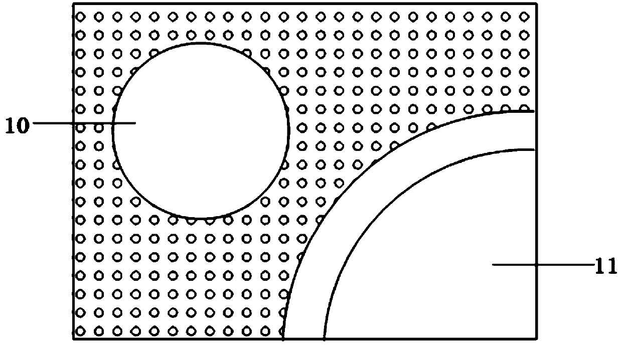
[0042] A UV LED chip with a p-type GaN layer, such as figure 1 As shown, it includes substrate 1, AlN buffer layer 2, non-doped AlGaN buffer layer 3, n-type AlGaN layer 4, quantum well layer 5, electron blocking layer 6, p-type GaN layer 7, A transparent conductive film layer 8 and a passivation layer 9, the transparent conductive film layer 8 is provided with a p-type ohmic electrode 9, the n-type AlGaN layer 4 is provided with an N-type ohmic electrode 11, and the p-type GaN layer 7 is uniformly etched with cylindrical body. The schematic diagram of the structure of the etched cylinder on the p-type GaN layer 7 is as follows figure 2 shown.

[0043] The ratio of the surface area of ​​the cylinder to the surface area of ​​the p-type GaN layer 7 was 30%.

[0044] The diameter of the cross-sectional circle of the cylinders is 3 μm, and the distance between adjacent cylinders is 3 μm.

[0045] The quantum well layer 5 is Al x Ga 1-x N / Al y Ga 1-y N multi-quantum well ac...

Embodiment 2

[0051] According to the UV LED chip described in Embodiment 1, the difference lies in that the p-type GaN layer 7 is uniformly etched with cones.

Embodiment 3

[0053] According to the UV LED chip described in Embodiment 1, the difference is that trapezoids are evenly etched on the p-type GaN layer 7 .


PUM

PropertyMeasurementUnit
Diameteraaaaaaaaaa
Thicknessaaaaaaaaaa
Thicknessaaaaaaaaaa

Abstract

The invention relates to a UV LED chip of a P-type GaN layer and a preparation method thereof. The UV LED chip comprises a substrate, an AlN buffer layer, an undoped AlGaN buffer layer, an n-type AlGaN layer, a quantum well layer, an electron barrier layer, a p-type GaN layer, a transparent conductive film layer and a passivation layer, which are arranged in order from bottom to top. A p-type ohmic electrode is arranged on the transparent conductive film layer. An N-type ohmic electrode is arranged on the n-type AlGaN layer. A regular structure body or an irregular structure body is etched onthe p-type GaN layer. Ultraviolet light absorption of the p-type GaN layer is reduced. Ohmic contact between the p-type GaN layer and the transparent conductive film layer is preserved. The external quantum efficiency and the light-emitting power of a UV-LED are improved.

Description

technical field [0001] The invention relates to a p-type GaN layer UV LED chip and a preparation method thereof, belonging to the field of optoelectronic technology. Background technique [0002] In recent years, LED has gradually become one of the most valued light source technologies. On the one hand, LED has the characteristics of small size; on the other hand, LED has the power-saving characteristics of low current and low voltage drive; Strong anti-seismic ability, long life and many other advantages. Especially in the ultraviolet region, the AlGaN-based multi-quantum well ultraviolet LED has shown great advantages, and has become one of the hot spots in the development of ultraviolet optoelectronic devices. AlGaN-based multi-quantum well UV LED devices have broad application prospects. Ultraviolet light has great application value in screen printing, polymer curing, environmental protection, air and water purification, medical treatment and biomedicine, white light l...

Claims


Application Information

Patent Timeline
IPC IPC(8): H01L33/22H01L33/00
CPCH01L33/0075H01L33/22
Inventor 王成新吴向龙肖成峰徐现刚
Owner SHANDONG INSPUR HUAGUANG OPTOELECTRONICS
Why Eureka
Try Eureka