

Method for rapidly etching and analyzing chemical state of material interface elements by using X-ray photoelectron spectrometer
A technology of photoelectron energy spectroscopy and interface elements, which is applied to the analysis of materials, material analysis using wave/particle radiation, instruments, etc., can solve the problems of inability to achieve rapid analysis and cannot truly reflect the chemical state of chemical elements in the film layer, and achieve reduction Analyze overall time, effect of increasing etch speed
- Summary
- Abstract
- Description
- Claims
- Application Information
AI Technical Summary
Problems solved by technology
Method used
Image

Examples
specific Embodiment approach 1
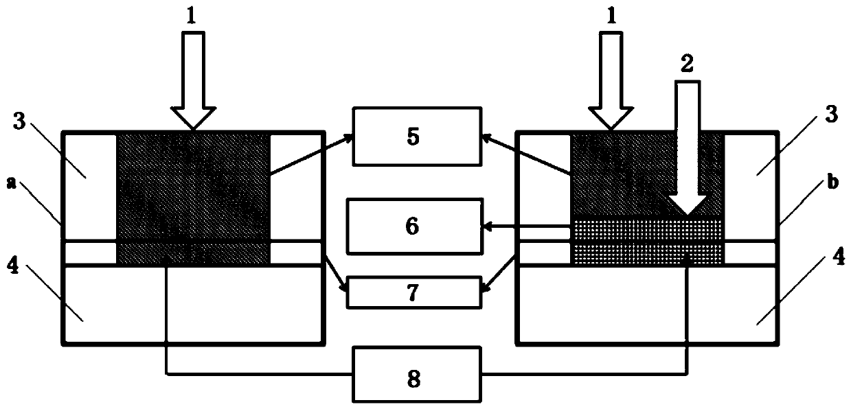
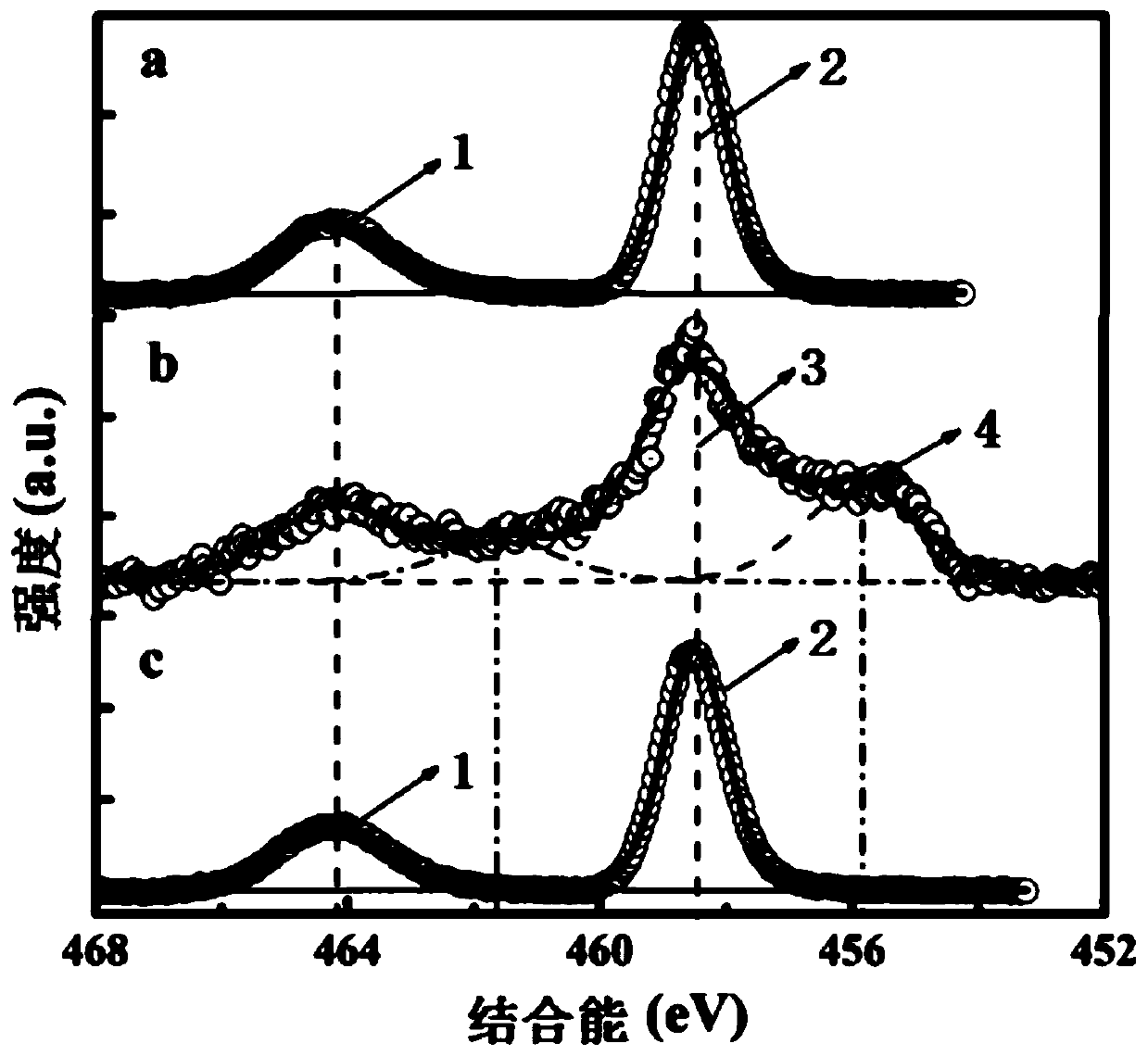
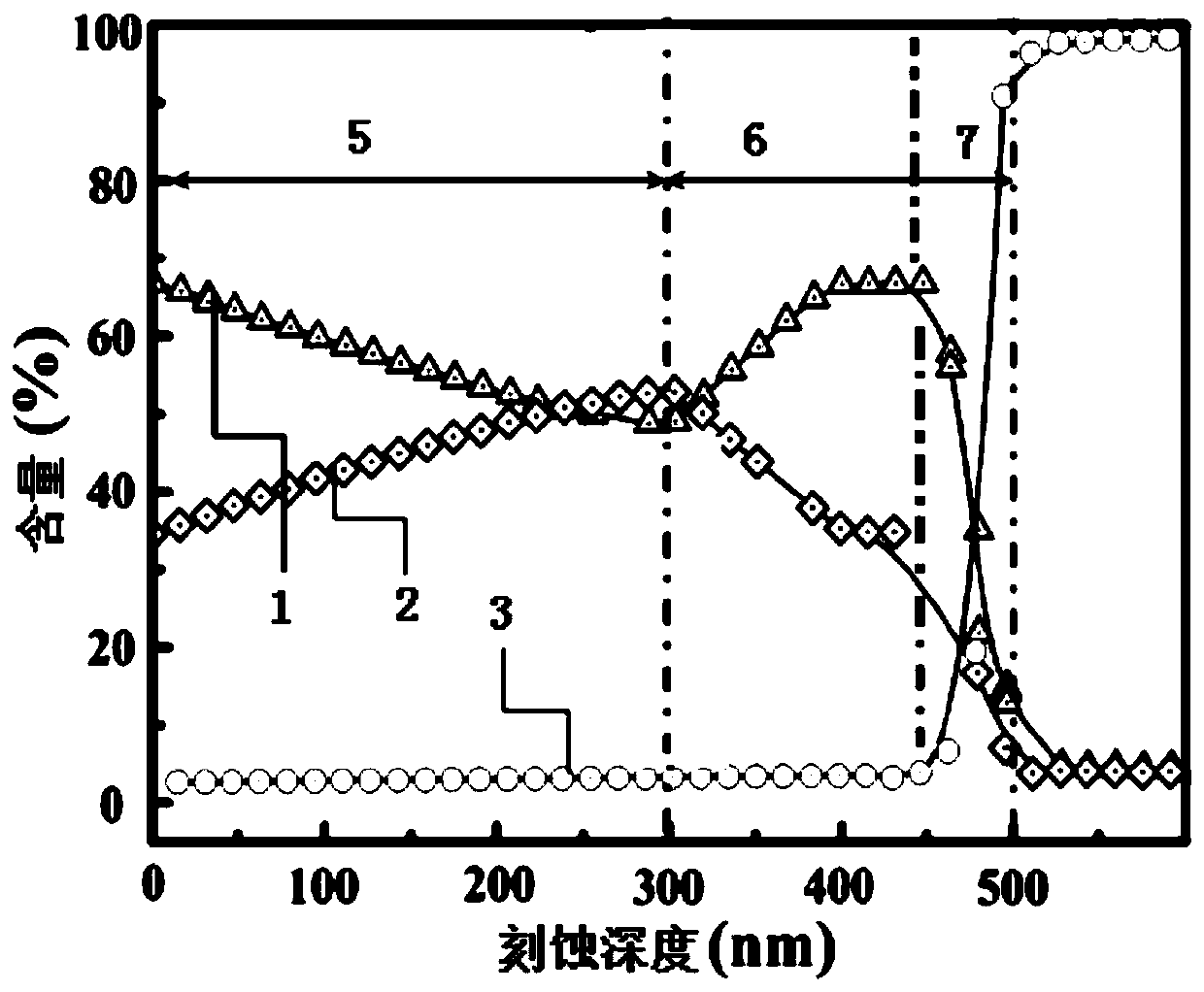
[0017] Specific Embodiment 1: This embodiment is a method for quickly etching and analyzing the chemical state of material interface elements using an X-ray photoelectron spectrometer. It is completed in the following steps:
[0018] 1. Remove the surface layer:
[0019] The material is placed in an X-ray photoelectron spectrometer, and the etching area is selected as 1mm 2 ~4mm 2 , under the condition that the etching rate is 0.05nm / s-0.2nm / s, use Ar ion etching in single-particle mode until the position is 100nm-200nm away from the interface layer;
[0020] The material is composed of n layers of films, n≥2, and n is a positive integer;
[0021] Or the material is a substrate with a film material on the surface, and the film material is composed of m layers of films, m≥1, and m is a positive integer;
[0022] Second, the interface layer analysis:
[0023] Under the condition of etching speed of 0.0005nm / s~0.001nm / s, use Ar ion in cluster mode to etch to the interface lay...
specific Embodiment approach 2
[0029] Embodiment 2: The difference between this embodiment and Embodiment 1 is that the energy of the single particle mode described in Step 1 is 1000 eV-4000 eV. Others are the same as the first embodiment.
specific Embodiment approach 3
[0030] Embodiment 3: This embodiment differs from Embodiment 1 or Embodiment 2 in that the energy of the cluster mode described in step 2 is 500 eV-4000 eV. Others are the same as those in Embodiment 1 or 2.
PUM
| Property | Measurement | Unit |
|---|---|---|
| thickness | aaaaa | aaaaa |
Abstract
Description
Claims
Application Information