A kind of h-3 silicon carbide isotope battery and its manufacturing method

An isotope battery, H-3 technology, applied in the direction of final product manufacturing, sustainable manufacturing/processing, circuits, etc., can solve the problems of shallow electron range, recombination loss of radiation-induced carriers, and difficulty in radiation-induced carrier loss. Avoid other problems, achieve wide depletion region thickness, improve energy conversion efficiency and packaging density, and have high promotion and application value

Active Publication Date: 2021-04-13
CHANGAN UNIV
View PDF10 Cites 0 Cited by
  • Summary
  • Abstract
  • Description
  • Claims
  • Application Information

AI Technical Summary

Problems solved by technology

[0005] However, there are still many problems in the research of silicon carbide PN-type isotope cells using H-3. The biggest problem is how to avoid the recombination loss of irradiated carriers on the surface of the device.
like image 3 As shown, the range of electrons generated by H-3 is relatively shallow, and the peak is close to the device surface, and the loss of radiation-induced carriers caused by surface recombination is unavoidable

Method used


Image

  • A kind of h-3 silicon carbide isotope battery and its manufacturing method
  • A kind of h-3 silicon carbide isotope battery and its manufacturing method
  • A kind of h-3 silicon carbide isotope battery and its manufacturing method

Examples


Embodiment 1

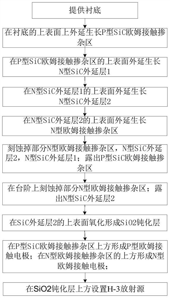
[0060] A kind of H-3 silicon carbide PN type isotope cell, comprises the following steps:

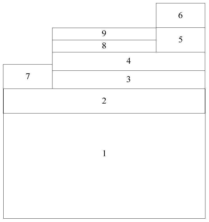
[0061] Step 1: providing an N-type doped SiC substrate (1);

[0062] Step 2: Using chemical vapor deposition to epitaxially grow on the upper surface of the substrate in Step 1 with a doping concentration of 1×10 19 cm -3 , a P-type SiC ohmic contact doped region (2) with a thickness of 1.0 μm;

[0063] Step 3: Using chemical vapor deposition to epitaxially grow the upper surface of the P-type SiC ohmic contact doped region (2) with a doping concentration of 4×10 17 cm -3 a first N-type SiC epitaxial layer (3) with a thickness of 1.0 μm;

[0064] Step 4: Using chemical vapor deposition to epitaxially grow the upper surface of the first N-type SiC epitaxial layer (3) with a doping concentration of 3×10 16 cm -3 , a second N-type SiC epitaxial layer (4) with a thickness of 0.5 μm;

[0065] Step 5: Using chemical vapor deposition to epitaxially grow the upper surface of the second N...


PUM

PropertyMeasurementUnit
thicknessaaaaaaaaaa
thicknessaaaaaaaaaa
thicknessaaaaaaaaaa

Abstract

The invention discloses a H-3 silicon carbide isotope battery and a manufacturing method thereof, comprising an N-type highly doped SiC substrate, a P-type SiC ohmic contact doping region, and a P-type SiC ohmic contact doping region from bottom to top. A first N-type SiC epitaxial layer is provided in a part of the upper part of the region, and a second N-type SiC epitaxial layer is arranged above the first N-type SiC epitaxial layer. In the upper part of the P-type SiC ohmic contact doped region, except for the first N-type SiC The region of the epitaxial layer is provided with a P-type ohmic contact electrode, and the upper part of the second N-type SiC epitaxial layer is provided with an N-type ohmic contact doped region, and an N-type ohmic contact electrode is provided above the N-type ohmic contact doped region. The area above the N-type SiC epitaxial layer except the N-type ohmic contact doped region is provided with SiO 2 passivation layer, on SiO 2 An H‑3 radioisotope source is provided above the passivation layer. The invention has a novel and reasonable design, can effectively solve the problem of recombination loss of H-3 irradiated carriers on the surface, and effectively improves the output power and energy conversion efficiency of the isotope battery.

Description

technical field [0001] The invention belongs to the technical field of semiconductor devices and semiconductor technology, and in particular relates to an H-3 silicon carbide isotope battery and a manufacturing method thereof. Background technique [0002] The isotope battery is an energy conversion device that converts nuclear radiation energy into electrical energy by using the radiovoltaic effect produced by charged particles produced by the decay of radioactive isotopes in semiconductor devices. Among many types of micro-energy sources, isotope batteries are regarded as the most ideal long-term energy sources for MEMS systems due to their high reliability, easy integration, and strong anti-interference. High output power is the prerequisite for the wide application of micronuclear batteries. However, due to the self-absorption effect and cost of isotope sources, it is difficult for micronuclear batteries to increase the output power by increasing the activity of the radi...

Claims


Application Information

Patent Timeline
Patent Type & Authority Patents(China)
IPC IPC(8): G21H1/06H01L31/068H01L31/18
CPCG21H1/06H01L31/068H01L31/1804Y02E10/547Y02P70/50
Inventor 张林朱礼亚王晓艳
Owner CHANGAN UNIV
Why Eureka
Try Eureka