Pixel structure of CMOS image sensor and forming method of pixel structure

An image sensor and pixel structure technology, applied in the field of image sensors, can solve problems such as the aperture ratio needs to be improved, and achieve the effect of improving the aperture ratio and quantum efficiency, and improving the signal-to-noise ratio

Inactive Publication Date: 2019-11-22
HUAIAN IMAGING DEVICE MFGR CORP
View PDF4 Cites 2 Cited by
  • Summary
  • Abstract
  • Description
  • Claims
  • Application Information

AI Technical Summary

Problems solved by technology

[0005] The fill factor (Fill Factor, FF) or aperture ratio of existing CMOS image sensor pixels still needs to be improved

Method used


Image

  • Pixel structure of CMOS image sensor and forming method of pixel structure
  • Pixel structure of CMOS image sensor and forming method of pixel structure
  • Pixel structure of CMOS image sensor and forming method of pixel structure

Examples


Embodiment Construction

[0041] As mentioned in the background, the aperture ratio (Fill Factor, FF) of the existing CMOS image sensor pixels still needs to be improved.

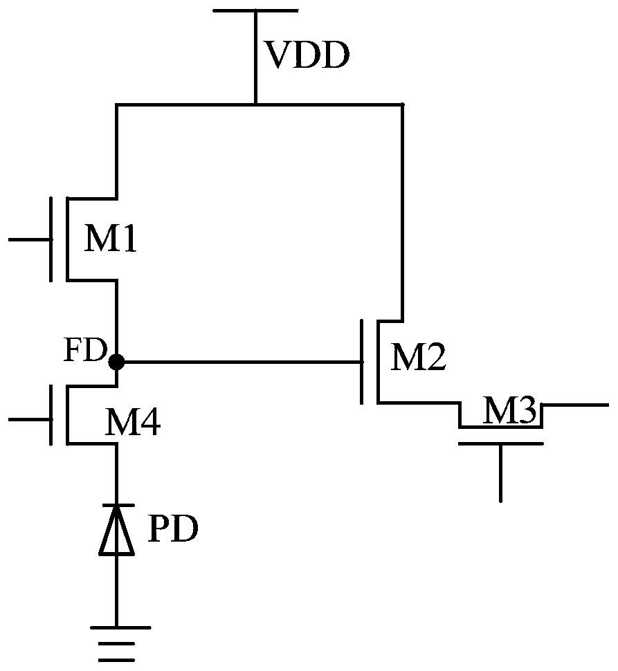
[0042]The study found that the pixel structure of the existing front-illuminated CMOS image sensor includes 1 photodiode and 4 transistors, and only the photodiode is used to sense light and generate photogenerated carriers. Therefore, the area of ​​the photodiode in the pixel structure occupies the entire pixel The ratio of the area of ​​the structure is directly related to the quantum efficiency and signal-to-noise ratio of the CMOS image sensor. The industry also refers to the ratio of the area of ​​the photodiode in the pixel structure to the area of ​​the entire pixel structure as the fill factor (FillFactor, FF) or aperture ratio. , the larger the fill factor (Fill Factor, FF) or aperture ratio, the higher the quantum efficiency and signal-to-noise ratio. The grid makes it difficult to further increase the fill factor (Fill Fa...


PUM


Abstract

The invention discloses a pixel structure of a CMOS image sensor and a forming method of the pixel structure, and the forming method comprises the steps: forming a floating diffusion region and a photodiode region located at one side of the floating diffusion region in a semiconductor substrate, wherein the depth of the photodiode region is greater than the depth of the floating diffusion region;etching a part of the photodiode region, and forming a groove in the photodiode region, wherein the depth of the groove is less than that of the photodiode region and greater than that of the floatingdiffusion region, and the side wall of the groove exposes the floating diffusion region; forming gate dielectric layers on the side wall and the bottom surface of the groove; and forming a transparent gate electrode on the surface of each gate dielectric layer, wherein the grooves are filled with the transparent gate electrodes. The aperture opening ratio and the quantum efficiency of the CMOS image sensor are improved.

Description

technical field [0001] The invention relates to the field of image sensors, in particular to a pixel structure of a CMOS image sensor and a forming method thereof. Background technique [0002] Image sensors are divided into complementary metal oxide (CMOS) image sensors and charge-coupled device (CCD) image sensors, which are generally used to convert optical signals into corresponding electrical signals. The advantage of the CCD image sensor is that it has high image sensitivity and low noise, but it is difficult to integrate the CCD image sensor with other devices, and the power consumption of the CCD image sensor is relatively high. In contrast, CMOS image sensors have the advantages of simple process, easy integration with other devices, small size, light weight, low power consumption, and low cost. At present, CMOS image sensors have been widely used in still digital cameras, camera phones, digital video cameras, medical imaging devices (such as gastroscopes), and aut...

Claims


Application Information

Patent Timeline
IPC IPC(8): H01L27/146
CPCH01L27/14605H01L27/14643H01L27/14683
Inventor 杨龙康林宗德黄仁德
Owner HUAIAN IMAGING DEVICE MFGR CORP
Why Eureka
Try Eureka