CMOS image sensor, pixel unit and control method thereof

An image sensor and pixel unit technology, applied in the field of image sensors, can solve the problem that the global exposure structure does not have a high dynamic range, and achieve the effect of high dynamic range and extended dynamic range

Active Publication Date: 2019-11-22
BRIGATES MICROELECTRONICS KUNSHAN
View PDF10 Cites 6 Cited by
  • Summary
  • Abstract
  • Description
  • Claims
  • Application Information

AI Technical Summary

Problems solved by technology

[0010] However, the global exposure structure including two-stage source follower does not have high dynamic range

Method used


Image

  • CMOS image sensor, pixel unit and control method thereof
  • CMOS image sensor, pixel unit and control method thereof
  • CMOS image sensor, pixel unit and control method thereof

Examples


Embodiment Construction

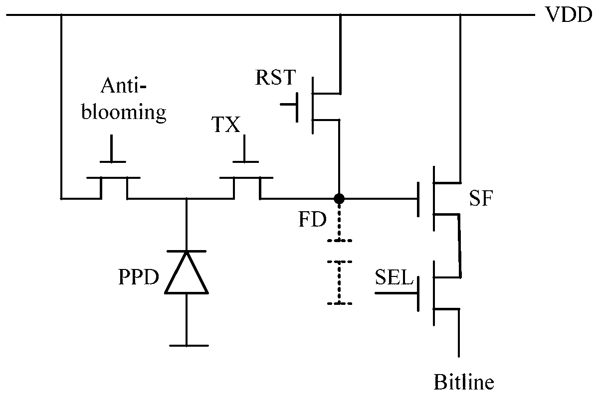
[0054] Existing global exposure structures including two-stage source followers (such as 8T type global exposure structure and 9T type global exposure structure) do not have a high dynamic range, and their dynamic range can only reach about 50 dB.

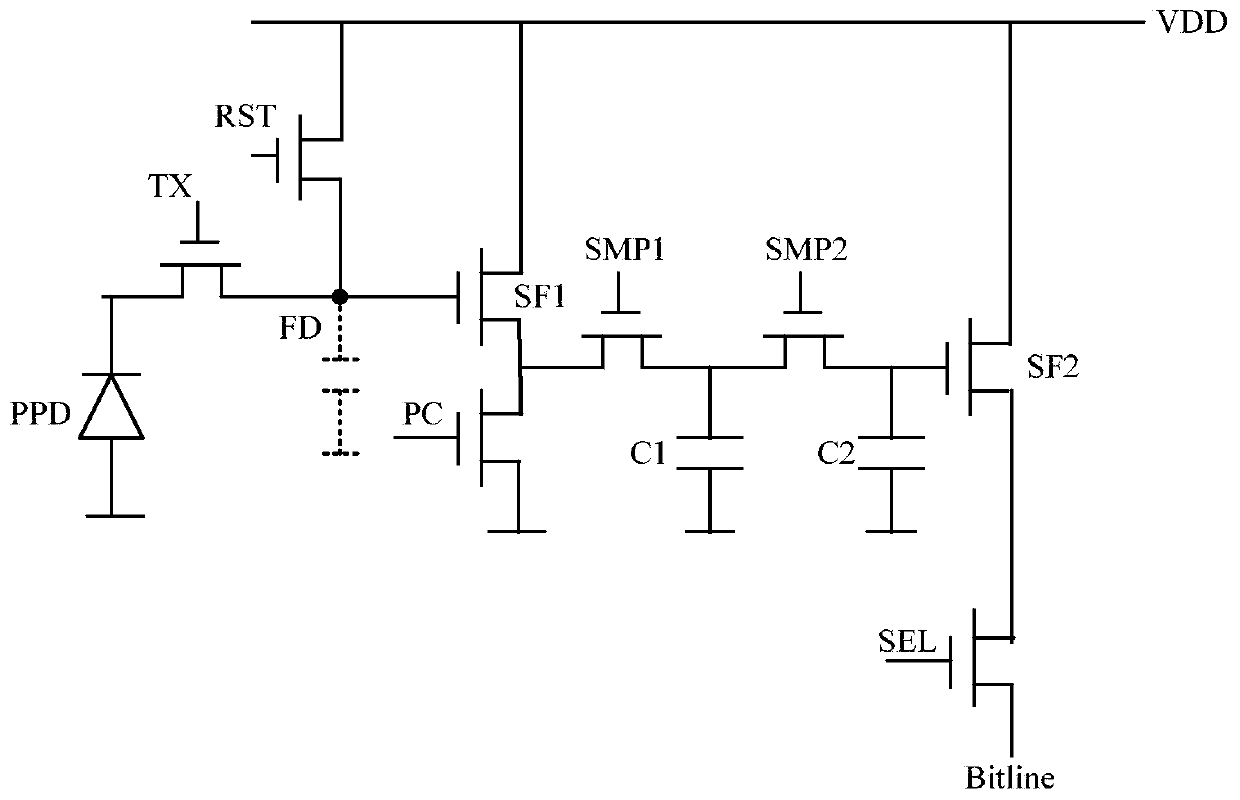
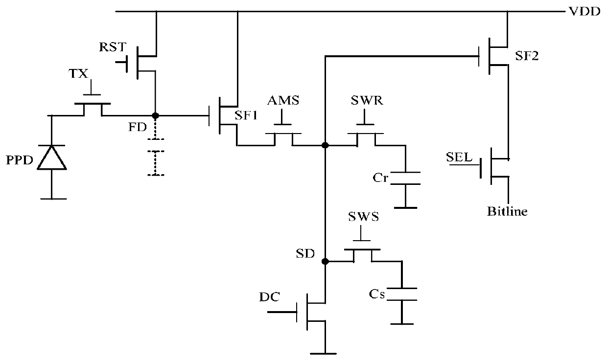
[0055] The technical solution of the present invention takes into account two characteristics of the storage node FD (for example, the capacitance C of the storage node FD FD The smaller the signal-to-noise ratio, the better, but the corresponding Q pd The smaller it is, the lower the dynamic range), and then provide two types of storage nodes, wherein the storage node with a smaller capacitance (Small FD, referred to as "SFD"; as known in the art, it belongs to parasitic capacitance, See Figure 1-3 The capacitance shown by the dotted line in the middle) is coupled to the first-stage source follower, and the storage node with a larger capacitance (Large FD, referred to as "LFD") is arranged in the overflow structure (the overflow...


PUM


Abstract

The invention discloses a CMOS image sensor, a pixel unit and a control method of the pixel unit. Each pixel unit comprises a global exposure structure, an overflow structure and a frame processing module. The overflow structure comprises a second transmission transistor, a second storage node and an overflow control transistor; the first end of the second transmission transistor is coupled with the cathode end of the photoelectric conversion element, and the second end is coupled with the first end of the second storage node; the second end of the second storage node is coupled with the firstpower line; the first end of the overflow control transistor is coupled to the second end of the second transmission transistor, and the second end is coupled to the gate of the second-stage source follower. The frame processing module quantizes the first frame analog signal and obtains first frame quantized data based on the quantized first frame analog signal, quantizes the second frame analogsignal and obtains second frame quantized data based on the quantized first frame analog signal, and adds the first frame quantized data and the second frame quantized data to obtain final quantized data. According to the technical scheme, the dynamic range of the pixel unit is expanded.

Description

technical field [0001] The invention relates to the technical field of image sensors, in particular to a CMOS image sensor, a pixel unit and a control method thereof. Background technique [0002] The image quality produced by the CMOS image sensor depends on the signal-to-noise ratio of the image signal, in which the signal intensity depends on the light intensity, exposure time, photoelectric conversion efficiency, etc. The noise mainly includes solid noise and random noise, and random noise includes shot noise and reset noise etc. [0003] The dynamic range of a CMOS image sensor is the ratio of the brightest signal to noise that the sensor can quantify. The lower limit of the dynamic range is determined by the noise. ), bitline (Bitline) swing, storage node (also known as floating diffusion area, Floating Diffusion, referred to as "FD") size and other factors, among which the Bitline swing is about 1V-1.5V, which is limited by the later terminal analog circuit design. ...

Claims


Application Information

Patent Timeline
IPC IPC(8): H04N5/374H04N5/355H04N5/357H04N5/363
CPCH04N25/57H04N25/616H04N25/65H04N25/76
Inventor 张琦
Owner BRIGATES MICROELECTRONICS KUNSHAN
Why Eureka
Try Eureka