

Two-dimensional material transistor based on a two-dimensional electron gas controllable back gate, manufacturing method and application
A technology of two-dimensional electron gas and two-dimensional materials, which is applied in the field of semiconductor electronic devices, can solve the problems of transistors, such as strict requirements on gate dielectric materials, poor repeatability, and large parasitic capacitance, so as to reduce device complexity and manufacturing costs, and achieve overall Simplified structure growth and reduced conduction loss
- Summary
- Abstract
- Description
- Claims
- Application Information
AI Technical Summary
Problems solved by technology
Method used
Image

Examples
preparation example Construction
[0062] Further, the preparation method of the two-dimensional material transistor based on the two-dimensional electron gas regulation back gate specifically includes: after the gate is fabricated on the heterojunction, rapid annealing is performed on the formed device structure, and the annealing temperature is 500 -1000°C, the time is 0.1-100min, so that an ohmic contact is formed between the gate and the two-dimensional electron gas or two-dimensional hole gas.
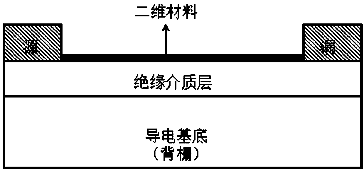
[0063] Further, the preparation method of the two-dimensional material transistor based on the two-dimensional electron gas regulation back gate specifically includes: forming an insulating dielectric layer on the second semiconductor, and then fabricating and forming the source on the insulating dielectric layer pole, drain.
[0064] Furthermore, the preparation method of the two-dimensional material transistor based on the two-dimensional electron gas regulation back gate specifically includes:
[0065] Transfer...
Embodiment 1
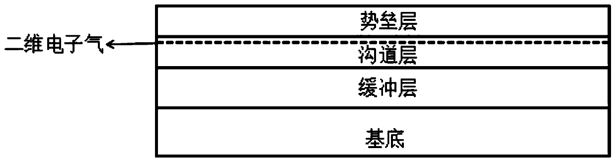
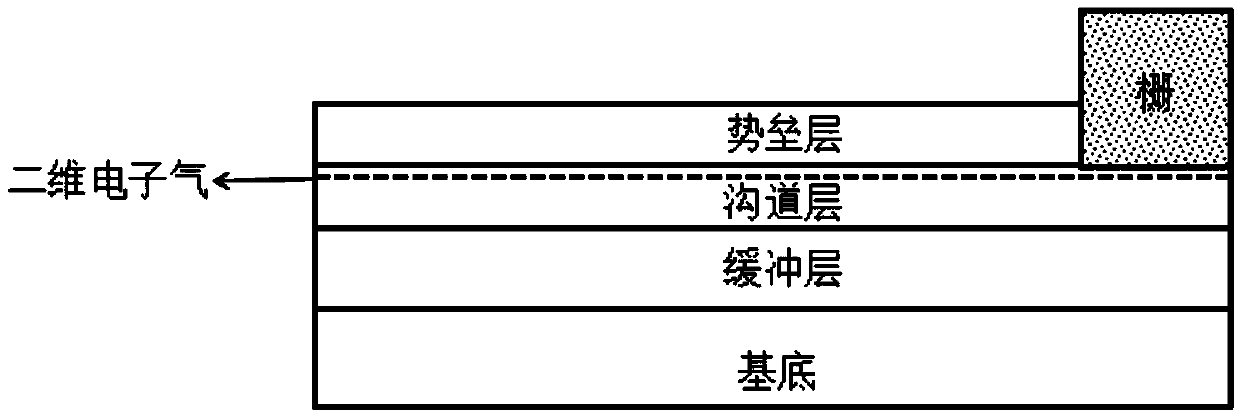
[0090] The structure of a two-dimensional material transistor based on a two-dimensional electron gas regulation back gate provided by this embodiment can be as follows Figure 6 As shown, it may include a buffer layer, a channel layer (also referred to as the first semiconductor), and a barrier layer (also referred to as the second semiconductor) sequentially arranged on the substrate, and the barrier layer is arranged at intervals There are source and drain, the source and drain are electrically connected by two-dimensional material, the gate is electrically connected with two-dimensional electron gas, the two-dimensional electron gas is formed in the heterogeneous layer composed of channel layer and barrier layer In the end.
[0091] A method for preparing a two-dimensional material transistor based on a two-dimensional electron gas regulation back gate provided in this embodiment may include the following steps:
[0092] 1) Using epitaxy techniques such as metal organic c...
Embodiment 2
[0100] Example 2: The structure of a two-dimensional material transistor based on a two-dimensional electron gas controlled back gate provided in this example can be found in Figure 7 As shown, the difference between it and the two-dimensional material transistor in Embodiment 1 is that an insulating dielectric layer is provided on the barrier layer, and the source, two-dimensional material, and drain are all disposed on the insulating dielectric layer.
[0101] The preparation method of the two-dimensional material transistor provided by this embodiment is basically the same as that of Embodiment 1, the difference is that: Step 1) also includes forming an insulating dielectric layer on the barrier layer, and using reactive ion etching or wet etching, etc. The etching method etches and removes the insulating dielectric layer in the area below the gate electrode, and then deposits the gate metal; or step 2) also includes, after forming the gate electrode, atomic layer depositio...
PUM
 Abstract
Description
Claims
Application Information