A use of sio 2 Method for preparing nonpolar a-plane gan epitaxial layer as substrate

An epitaxial layer, non-polar technology, applied in the field of semiconductor material preparation, can solve the problem of high cost of non-polar GaN

Active Publication Date: 2021-05-11
TAIYUAN UNIV OF TECH
View PDF8 Cites 0 Cited by
  • Summary
  • Abstract
  • Description
  • Claims
  • Application Information

AI Technical Summary

Problems solved by technology

Using sapphire, LiAlO 2 The cost of preparing non-polar GaN with SiC and other substrates is high, and the film quality needs to be further improved

Method used


Image

  • A use of sio  <sub>2</sub> Method for preparing nonpolar a-plane gan epitaxial layer as substrate
  • A use of sio  <sub>2</sub> Method for preparing nonpolar a-plane gan epitaxial layer as substrate
  • A use of sio  <sub>2</sub> Method for preparing nonpolar a-plane gan epitaxial layer as substrate

Examples


Embodiment 1

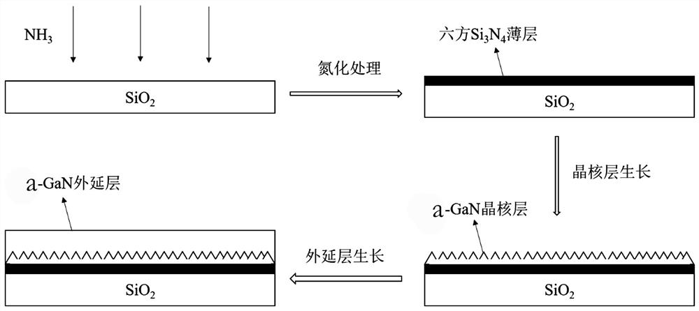
[0018] Embodiment 1: a kind of SiO 2 As a method for preparing a non-polar a-plane GaN epitaxial layer as a substrate, the SiO 2 The substrate is nitrided at a high temperature of 1200-1300°C and a large ammonia gas flow rate of 4000-4500 sccm. After the treatment, SiO 2 a-Si with close-packed hexagonal structure formed on the substrate surface 3 N 4 Thin layer; a-plane oriented GaN crystal nucleus layer is grown on the thin layer, and finally a-plane GaN epitaxial layer is grown on the basis of non-polar crystal nucleus.

[0019] Specific steps are as follows:

[0020] (1) SiO 2 Substrate surface clean, nitriding treatment: SiO 2 The substrate was placed in a metal-organic vapor deposition (MOCVD) reaction chamber, and the substrate was cleaned at a temperature of 1250 °C under a hydrogen atmosphere; Pressure 150 mbar; SiO after nitriding 2 A layer of a-Si with hexagonal close-packed structure will be formed on the surface of the substrate. 3 N 4 Thin layer with a th...

Embodiment 2

[0024] Embodiment 2: a kind of in SiO 2 The method for preparing a nonpolar a-plane GaN epitaxial layer from a substrate, the specific steps are as follows:

[0025] (1) SiO 2 Substrate surface clean, nitriding treatment: SiO 2 The substrate was placed in a metal-organic vapor deposition (MOCVD) reaction chamber, and the substrate was cleaned at a temperature of 1300 ° C under a hydrogen atmosphere; The chamber pressure is 200 mbar; after nitriding SiO 2 A layer of a-Si with hexagonal close-packed structure will be formed on the surface of the substrate. 3 N 4 Thin layer with a thickness of 10nm;

[0026] (2) Growth of a-plane GaN crystal nucleus layer: after step (1), lower the temperature to 1050 °C, feed 50 sccm gallium source and 400 sccm ammonia gas into the reaction chamber, the V / III ratio is 200, and the reaction pressure Grow for 35 s under the condition of 200 mbar to generate a-plane GaN crystal nucleus layer;

[0027] (3) Growth of a-plane GaN epitaxial layer:...

Embodiment 3

[0028] Embodiment 3: a kind of in SiO 2 The method for preparing a nonpolar a-plane GaN epitaxial layer from a substrate, the specific steps are as follows:

[0029] (1) SiO 2 Substrate surface clean, nitriding treatment: SiO 2 The substrate was placed in a metal-organic vapor deposition (MOCVD) reaction chamber, and the substrate was cleaned at a temperature of 1200 °C under a hydrogen atmosphere; The chamber pressure is 100 mbar; after nitriding SiO 2 A layer of a-Si with hexagonal close-packed structure will be formed on the surface of the substrate. 3 N 4 Thin layer with a thickness of 6nm;

[0030] (2) Growth of a-plane GaN crystal nucleus layer: after step (1), lower the temperature to 1100 °C, feed 45 sccm gallium source and 300 sccm ammonia gas into the reaction chamber, keep the V / III ratio at 150, and keep the pressure at Grow for 45 s under the condition of 100 mbar to generate a-plane GaN crystal nucleus layer;

[0031] (3) Growth of a-plane GaN epitaxial la...


PUM

PropertyMeasurementUnit
thicknessaaaaaaaaaa

Abstract

The invention belongs to the technical field of semiconductor material preparation, and provides a metal organic compound chemical vapor deposition (MOCVD) process on SiO 2 A method for preparing a nonpolar a-plane GaN epitaxial layer from a substrate. SiO 2 The substrate is nitrided at 1200‑1300°C under the condition of high temperature and large ammonia gas flow rate of 4000‑4500 sccm. After the treatment, SiO 2 a-Si with close-packed hexagonal structure formed on the substrate surface 3 N 4 Thin layer; a-plane oriented GaN crystal nucleus layer is grown on the thin layer, and finally a-plane GaN epitaxial layer is grown on the basis of non-polar crystal nucleus. Compared with the widely used polar c-plane GaN, the non-polar a-plane GaN-based device eliminates the quantum confinement Stark effect caused by the polarization effect, has high internal quantum efficiency, and has no light emission at high current density. Advantages such as wavelength drift.

Description

technical field [0001] The invention belongs to the technical field of semiconductor material preparation, and in particular relates to a metal organic compound chemical vapor deposition (MOCVD) process to form SiO 2 A method for preparing a nonpolar a-plane GaN epitaxial layer from a substrate. Background technique [0002] Gallium nitride (GaN) material has the advantages of direct wide bandgap, stable chemical properties, high melting point (2300 ° C), etc., and has a wide range of applications in solid-state lighting, solar cells, sterilization, lasers, etc. GaN with a wurtzite structure is a non-centrosymmetric crystal, and its polar axis is the c-axis. Researchers generally epitaxially grow polar c-plane GaN films on polar c-plane sapphire substrates. However, there is a polarization electric field inside GaN on the polar plane. Under the action of the polarization electric field, the electrons and holes in the quantum well are separated in space, and the probability...

Claims


Application Information

Patent Timeline
Patent Type & Authority Patents(China)
IPC IPC(8): H01L21/02C30B25/18C30B29/40
CPCC30B25/183C30B29/406H01L21/02414H01L21/02488H01L21/0254H01L21/0262
Inventor 李天保张哲于斌贾伟余春燕董海亮贾志刚许并社
Owner TAIYUAN UNIV OF TECH
Why Eureka
Try Eureka