Silicon carbide LDMOS device suitable for monolithic integration and manufacturing method thereof

A technology of monolithic integration and silicon carbide, which is applied in semiconductor/solid-state device manufacturing, semiconductor devices, electrical components, etc., can solve the problems of high price of semi-insulating substrates and difficult preparation of P-type substrates, and achieve low cost and low cost. The effect of on-resistance

Active Publication Date: 2019-11-29
SOUTH UNIVERSITY OF SCIENCE AND TECHNOLOGY OF CHINA
View PDF5 Cites 10 Cited by
  • Summary
  • Abstract
  • Description
  • Claims
  • Application Information

AI Technical Summary

Problems solved by technology

[0004] Generally, LDMOS devices used in silicon integrated circuits use P-type substrates or SOI silicon substrates. For silicon carbide materials, P-type substrates are extremely difficult to prepare, and the price of semi-insulating substrates is relatively high.

Method used


Image

  • Silicon carbide LDMOS device suitable for monolithic integration and manufacturing method thereof
  • Silicon carbide LDMOS device suitable for monolithic integration and manufacturing method thereof
  • Silicon carbide LDMOS device suitable for monolithic integration and manufacturing method thereof

Examples


Embodiment 1

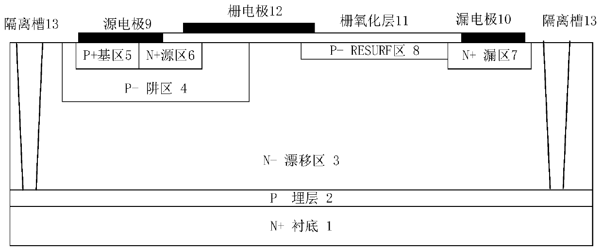
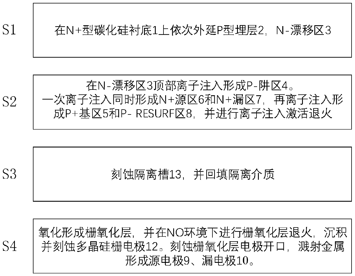
[0030] An aspect of the embodiments of the present invention provides a silicon carbide LDMOS device structure, figure 1 It is a schematic diagram of the structure of the silicon carbide LDMOS device of the present invention. Such as figure 1 As shown, the device structure includes an N-type highly doped substrate 1 , above which is a P-type epitaxial isolation buried layer 2 and an N-type lightly doped drift region 3 . On top of the drift region 3, a P-well region 4, a P+ base region 5, an N+ source region 6, a P-RESURF region 8 and an N+ drain region 7 are distributed. Wherein, the P+ base region 5 and the N+ source region 6 are located inside the P-well region 4, and there is a gap with a certain width between the N+ drain region and the P-well region, and the gap width depends on the blocking voltage set in the device design. Between the P- well region and the N+ drain region is the P-RESURF region 8 , which is close to the N+ drain region 7 . Above the drift region 3 i...

Embodiment 2

[0048] The embodiment of the present invention provides another basic structure of silicon carbide LDMOS, the basic structure of which is as follows Figure 8 shown. The difference from the structure provided in Embodiment 1 is that the P-RESURF region 8 is replaced by the segmented P-region 8, which can obtain a more uniform lateral field drop, improve the blocking capability of the device, and reduce the on-resistance of the device.

Embodiment 3

[0050] The embodiment of the present invention provides a basic structure of a silicon carbide LDMOS, the basic structure of which is as follows Figure 9 shown. The difference from the structure provided in Embodiment 1 is that the P-type buried layer is divided into two parts: a highly doped P+ buried layer 22 and a lightly doped P− buried layer 21 . The doping concentration of P-buried layer 21 is 1×10 14 cm -3 to 1×10 16 cm -3 , the doping concentration of the P+ buried layer 22 is 1×10 14 cm -3 to 1×10 16 cm -3 , which can increase the breakdown voltage of the drain liner in the blocking state.


PUM


Abstract

The invention relates to the technical field of power semiconductors, and discloses a silicon carbide LDMOS device suitable for integration and a manufacturing method thereof. The device comprises anN-type highly doped substrate on which a P-type epitaxial isolation buried layer and an N-type light doped drift region are sequentially arranged. A P- well region, a P + base region, an N + source region, a P- RESURF region and an N + drain region are distributed on the top of the drift region, wherein the P + base region and the N + source region are located in the P- well region. The P- RESURFregion is arranged between the P- well region and the N + drain region and close to N + drain region. A gate oxide layer is arranged on the drift region and covers a channel region formed by nesting the P- well region and the N + source region and the P- RESURF region. The novel silicon carbide LDMOS device has the characteristics of high blocking voltage, low conduction resistance and the like, and the process is completely compatible with the current vertical structure silicon carbide MOSFET so as to facilitate preparation of the silicon carbide power integrated circuit. Meanwhile, the RESURF technology is introduced to the device so as to increase the breakdown voltage of the device and reduce the conduction resistance of the device.

Description

technical field [0001] The invention belongs to the technical field of semiconductor power devices, and in particular relates to a high-voltage silicon carbide LDMOS device and a manufacturing method. Background technique [0002] Silicon carbide material has excellent material properties and is considered to be the core material of next-generation power semiconductor technology. At present, silicon carbide JBS, MOSFET and other devices have been widely used in many fields such as new energy vehicles and electric energy conversion. However, in the field of power integrated circuits, the application of silicon carbide technology is still relatively rare. The main reason is that the defect density of silicon carbide is still relatively large, and suitable and easy-to-integrate lateral silicon carbide devices are still relatively scarce. [0003] LDMOS (Lateral Double Diffused Metal Oxide Field Effect Transistor) has the advantages of high gain, wide linear range, small distort...

Claims


Application Information

Patent Timeline
Patent Type & Authority Applications(China)
IPC IPC(8): H01L29/78H01L29/06H01L21/04
CPCH01L29/7816H01L29/063H01L21/0445H01L29/66068
Inventor 温正欣叶怀宇张国旗
Owner SOUTH UNIVERSITY OF SCIENCE AND TECHNOLOGY OF CHINA
Why Eureka
Try Eureka