High-efficiency crystalline silicon heterojunction solar cell silicon wafer cleaning device and method

A technology for cleaning solar cells and silicon wafers. It is used in the manufacture of circuits, electrical components, and semiconductor/solid-state devices.

Pending Publication Date: 2019-12-03
SUZHOU AIKANG LOW CARBON TECH INST
View PDF0 Cites 1 Cited by
  • Summary
  • Abstract
  • Description
  • Claims
  • Application Information

AI Technical Summary

Problems solved by technology

Without increasing water consumption and cleaning time, and without increasing manufacturing costs, the surface of silicon wafers after cleaning is cleaner, solving the problem of unclean silicon wafer surface cleaning in HJT cells, improving the photoelectric conversion efficiency of HJT solar cells, and at the same time stable The process is more suitable for mass production

Method used


Image

  • High-efficiency crystalline silicon heterojunction solar cell silicon wafer cleaning device and method
  • High-efficiency crystalline silicon heterojunction solar cell silicon wafer cleaning device and method
  • High-efficiency crystalline silicon heterojunction solar cell silicon wafer cleaning device and method

Examples


Embodiment 1

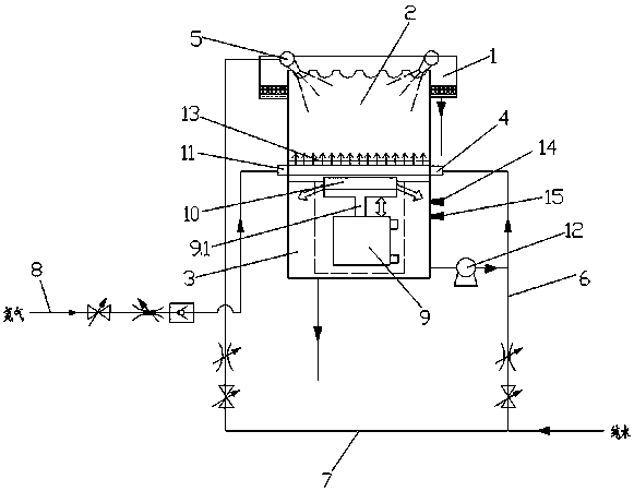
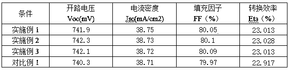
[0040] a. Adopt the above-mentioned cleaning method to carry out texturing and cleaning treatment to the N-type monocrystalline silicon wafer (180um) with a size of 156.75mm. The cleaning time is 50s for overflow and 70s for spraying;

[0041] b. The intrinsic amorphous silicon layer on the back is prepared by PECVD, and the 7nm deposition is completed in one step;

[0042] c. Selecting the n-type amorphous silicon film as the doped layer on the light-receiving surface. Using plasma-enhanced chemical vapor deposition to prepare an n-type amorphous silicon layer with a thickness of 6 nm;

[0043] d. Use plasma chemical vapor deposition to prepare a p-type amorphous silicon layer with a total thickness of 10 nm;

[0044] e. Use (RPD, PVD) method to deposit TCO conductive film with a thickness of 100nm;

[0045] f. Form front and back silver metal electrodes by screen printing;

[0046] g. Curing makes a good ohmic contact between the silver grid line and the TCO;

[0047] h....

Embodiment 2

[0049] Same as Example 1, except that the cleaning time is 70s for overflow and 50s for spraying.

Embodiment 3

[0051] Same as Example 1, except that the cleaning time is 90s for overflow and 30s for spraying.


PUM


Abstract

The invention relates to a high-efficiency crystalline silicon heterojunction solar cell silicon wafer cleaning device and method. The device comprises an overflow tank, and upper and lower tanks which are arranged above and below. A liquid inlet pipe and an air inlet pipe are arranged at the lower part of the upper tank. A pure water spray is arranged at the top. Pure water enters an overflow pipe and a spray pipe. Nitrogen enters a nitrogen pipe. The nitrogen pipe is connected with the inlet pipe. The overflow pipe is connected with the liquid inlet pipe. The spray pipe is connected with thepure water spray. A fast-discharging cylinder is arranged in the lower tank. The piston rod of the fast-discharging cylinder is connected with a fast-discharging cover. The upper tank is provided with a fast-discharging opening corresponding to the fast-discharging cover. According to the invention, water washing is divided into two steps of pure water overflow and spraying, so that the last water contacted by a silicon wafer is clean new pure water; the problem of uncleaned silicon wafer surface in an HJT cell is solved; the photoelectric conversion efficiency of the HJT solar cell is improved; and the stable process is more suitable for mass production.

Description

technical field [0001] The invention relates to the technical field of high-efficiency battery manufacturing in the photovoltaic industry, in particular to a silicon chip cleaning device and method for high-efficiency crystalline silicon heterojunction solar cells. Background technique [0002] During the preparation of HJT solar cells, texturing cleaning is the first process, which provides a clean crystalline silicon surface for the PECVD-prepared amorphous silicon layer, so texturing cleaning has a huge impact on the conversion efficiency of HJT cells. It is very important for the efficiency and stability of the battery. [0003] For HJT solar cells, the current cleaning process for texturing is as follows: feeding→pre-cleaning→rough polishing→water washing→texturing→water washing→alkaline cleaning→water washing→correction→water washing→pickling→water washing→acid cleaning→water washing→drying→ After each step of the functional tank, there will be a washing tank. Its f...

Claims


Application Information

Patent Timeline
Patent Type & Authority Applications(China)
IPC IPC(8): H01L21/67H01L21/02
CPCH01L21/02052H01L21/02057H01L21/02082H01L21/67023H01L21/6704H01L21/67051
Inventor 凌俊易治凯郭小勇王永谦
Owner SUZHOU AIKANG LOW CARBON TECH INST
Why Eureka
Try Eureka