Full-MOS voltage and temperature monitoring method and circuit

A technology for monitoring circuits and voltages, which is applied in the field of full MOS voltage and temperature monitoring methods and circuits, can solve problems such as poor practicability, high cost, and poor practicability, and achieve improved range and accuracy, no static power consumption, and simple structure Effect

Active Publication Date: 2019-12-06
广州粒子微电子有限公司
View PDF16 Cites 5 Cited by
  • Summary
  • Abstract
  • Description
  • Claims
  • Application Information

AI Technical Summary

Problems solved by technology

[0008] In the Chinese patent application document with the publication number CN101751062A, the temperature drift of the ring oscillator is compensated by a low-noise reference voltage generation circuit and a linear regulator. However, the circuit structure is complex, and trimming resistors are used. The manufacturing process is complicated and the cost is high.
[0009] In the Chinese patent application document with the publication number CN103684354A, two kinds of inverters with positive and negative temperature coefficients are used to form a ring oscillator. Although the problem of temperature drift is solved, the dispersion caused by the process is not considered, and the practicability is poor.
[0010] From the above examples, it can be seen that the design realized in the all-digital process often lacks comprehensive compensation for PVT, resulting in poor practicability; while the design that considers PVT compensation mostly uses additional analog devices, resulting in inability to fully digital

Method used


Image

  • Full-MOS voltage and temperature monitoring method and circuit
  • Full-MOS voltage and temperature monitoring method and circuit
  • Full-MOS voltage and temperature monitoring method and circuit

Examples


no. 1 example

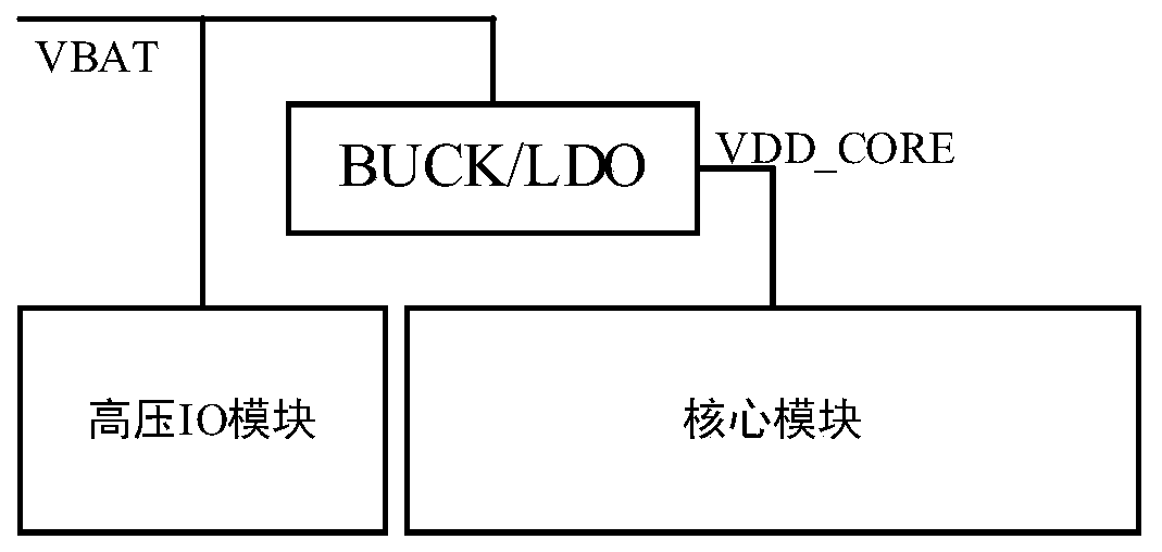
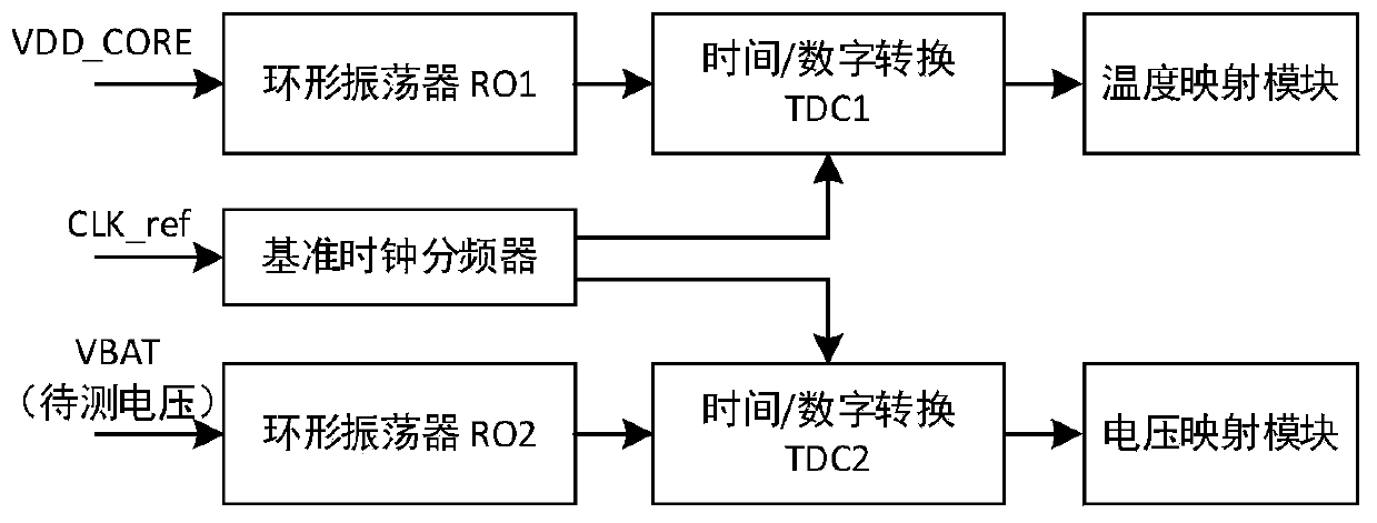
[0050] Based on the above-mentioned power supply system, the schematic diagram of the present invention is as follows figure 2 As shown, it includes two ring oscillators RO1 and RO2, two time / digital converters TDC1 and TDC2, a temperature mapping module, a voltage mapping module and a reference clock divider module. Wherein, the reference clock may be a system reference clock provided by a crystal oscillator, the ring oscillator RO1 is powered by the core domain power supply voltage VDD_CORE, and the ring oscillator RO2 is powered by the battery voltage VBAT. The reference clock is respectively connected to TDC1 and TDC2 after the reference clock frequency divider, and the output terminals of TDC1 and TDC2 are respectively connected to the temperature mapping module and the voltage mapping module.

[0051] Due to the carrier mobility μ of the MOS tube n , saturated drain-source voltage V dsat and threshold voltage V th Parameters such as process (Process), voltage (Voltag...

no. 2 example

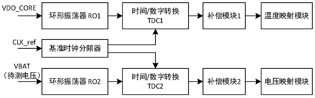
[0086] The description of the first embodiment is based on the condition that the chip production process parameters do not deviate. If there is a deviation in the process parameters, a compensation module needs to be used to compensate the temperature and voltage. Therefore, the second embodiment of the present invention adds a temperature compensation module 1 and a voltage compensation module 2, and uses the compensation module 1 and the compensation module 2 to respectively compensate the digital values ​​X1 and X2 corresponding to the temperature and voltage to obtain accurate temperature and voltage value. It is another embodiment of the present invention, such as image 3 shown. In addition, the compensation module also has a compensation function for temperature nonlinearity and voltage nonlinearity.

[0087] For the calibration of process deviation: Since the process deviation will cause changes in f0, Kvco and TC, the count value obtained by counting will change. ...

no. 3 example

[0091] In the second embodiment, in order to compensate the variation of the process deviation, we adopt the method of multiplying the difference of the count value by a compensation coefficient. It can be seen from the formula that another compensation method is to change the counting cycle K to get the same effect. By changing the frequency division ratio of the programmable frequency divider, the number of counting cycles K can be changed to compensate for changes in process deviations.


PUM


Abstract

The invention provides a full-MOS voltage and temperature monitoring method and monitoring circuit. The circuit comprises two annular oscillators RO1 and RO2, two time-digital converters TDC1 and TDC2, a temperature mapping module, a voltage mapping module, a reference clock frequency divider module and two compensation modules, wherein a reference block is provided by a crystal oscillator, poweris supplied to the annular oscillator RO1 through a core-domain power supply voltage VDD_CORE, power is supplied to the annular oscillator RO2 through a battery voltage VBAT, the reference clock is separately connected to the TDC1 and the TDC2 through the frequency divider, and output terminals of the TDC1 and the TDC2 are respectively connected to the temperature mapping module and the voltage mapping module. According to the method and circuit, real full MOS can be realized, extra masks are avoided, effective calibration of the PVT is realized, the monitoring precision is improved, and the method and the circuit are advantageous in that the structure is simple, the area is small, and static power consumption is avoided.

Description

technical field [0001] The invention relates to the field of chip design, in particular to a full MOS voltage and temperature monitoring method and circuit in the chip. Background technique [0002] In an integrated circuit, it is particularly important to monitor the power supply voltage and temperature of the chip. On the one hand, due to the limitation of the withstand voltage of the process, too high power supply voltage will reduce the working life of the chip, and even cause permanent damage to the chip device; on the other hand, too low power supply voltage may affect the function of the chip, resulting in erroneous operation of the system . In addition, due to the sensitivity of semiconductor devices to temperature, when the temperature exceeds a certain range, the normal operation of the chip may be affected. Therefore, it is necessary to monitor the temperature of the chip, and perform necessary temperature compensation on the chip as required, so as to ensure th...

Claims


Application Information

Patent Timeline
Patent Type & Authority Applications(China)
IPC IPC(8): G01R31/317G01R31/40G01K13/00G01R35/00
CPCG01K13/00G01R31/31704G01R31/31721G01R31/31725G01R31/40G01R35/005G01R35/007
Inventor 徐肯
Owner 广州粒子微电子有限公司
Why Eureka
Try Eureka