MPCVD (microwave plasma chemical vapor deposition) device

A technology of chemical vapor deposition and microwave plasma, which is applied in the direction of chemical reactive gas, gaseous chemical plating, chemical instruments and methods, etc., can solve the problem of uneven gas distribution on the surface of the sample table, poor focusing ability, and dielectric window etching and other problems to achieve the effect of solving the problem of plasma etching

Active Publication Date: 2019-12-13
广东众元半导体科技有限公司
View PDF16 Cites 3 Cited by
  • Summary
  • Abstract
  • Description
  • Claims
  • Application Information

AI Technical Summary

Problems solved by technology

[0010] The purpose of the present invention is to propose a microwave plasma chemical vapor deposition device, which overcomes the problems existing in the existing devices to varying degrees: diele

Method used


Image

  • MPCVD (microwave plasma chemical vapor deposition) device
  • MPCVD (microwave plasma chemical vapor deposition) device
  • MPCVD (microwave plasma chemical vapor deposition) device

Examples


Embodiment 1

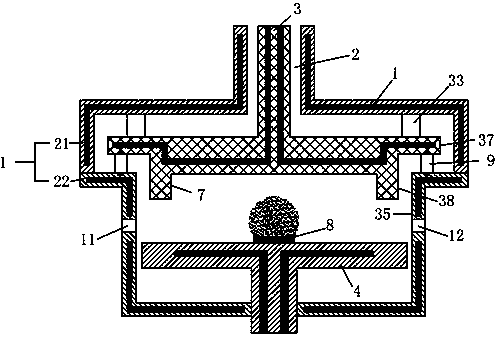
[0033] Such as figure 1 As shown, a microwave plasma chemical vapor deposition device of the present invention includes: the reaction chamber 1 includes an upper chamber 21 and a lower chamber 22, the bottom of the reaction chamber 1 is provided with a sample stage 4 for placing a substrate 8, and the reaction chamber 1 The top is provided with a central axis 3, the reaction chamber 1 and the central axis 3 form a quasi-coaxial waveguide 2, the central axis 3 extends into the reaction chamber, and the side of the central axis facing the sample stage 4 is provided with a concave structure surface 7; the reaction chamber 1. A horizontal air inlet 11 and a horizontal air outlet 12 are provided; in the coaxial waveguide 2, a sealing insulating member 9 and an insulating support member 33 are arranged; the lower end surface of the central axis 2 is lower than the sealing The lower end surface of the insulating member 9 and the lower end surface of the insulating support member 33; ...

Embodiment 2

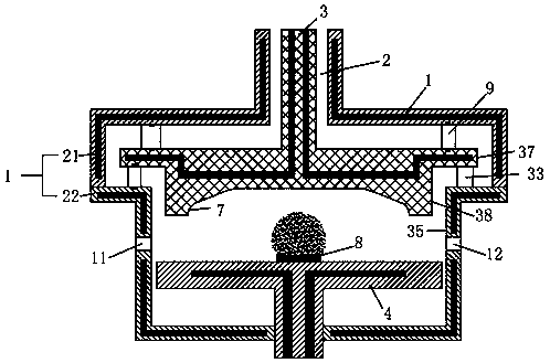
[0039] Such as figure 2 As shown, the concave structure surface 7 of the central axis 3 adopts a cylindrical concave surface, and many chamfers and fillets are added to the cylindrical concave surface 7 . Meanwhile, the sealing insulating part 9 is located between the central shaft 3 and the upper cavity 21 , and the insulating support 33 is located between the central shaft 3 and the lower cavity 22 . These two points are the differences between this embodiment and Embodiment 1.

[0040] The change of the shape of the surface 7 of the concave structure has a certain influence on the electric field intensity and the plasma density above the center of the sample stage 4 .

[0041] The sealing insulator 9 is positioned between the central shaft 3 and the upper cavity 21, and the insulating support 33 is positioned between the central shaft 3 and the lower cavity 22, and the pre-loaded compression force is also sufficient when there is no vacuum in the cavity. Sufficient for a...

Embodiment 3

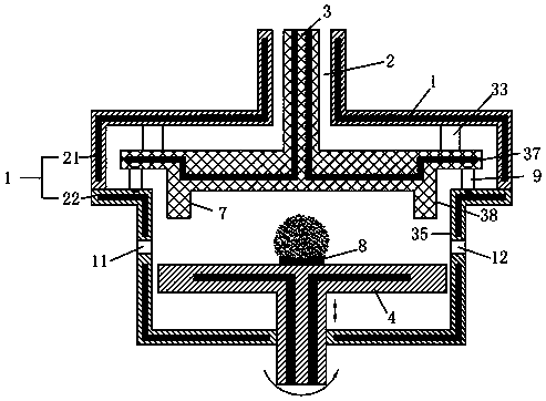
[0043] Such as image 3 As shown, the sample stage 4 can be adjusted up and down, and can be rotated. These two points are the differences between this embodiment and embodiment 1. The up and down adjustment of the sample stage 4 can adjust the resonant frequency of the reaction chamber 1 and can adjust the form of the plasma. The sample stage 4 can be rotated, and the gas flow rate of the gas inlet 11 is matched with the rotation speed of the sample stage 4, which can realize the homogenization of the reaction gas on the surface of the substrate 8, and can better realize the uniform growth of the diamond film, especially for large-area substrates. The doping uniformity of the bottom, the improvement effect is more obvious.


PUM


Abstract

The invention discloses an MPCVD (microwave plasma chemical vapor deposition) device. The MPCVD device comprises an upper cavity, a lower cavity, a center shaft, a sample table, sealed insulating parts, insulated supporting parts, a gas inlet and a gas outlet, wherein the center shaft is arranged above a reaction cavity and forms a coaxial waveguide allowing microwave feed-in with the reaction cavity; the sample table arranged below the reaction cavity is used for substrate placement, and the center shaft facing one side of the sample table is provided with a sunken structure surface; the sealed insulating parts and the insulated supporting parts are arranged in the coaxial waveguide, meanwhile, the lower end surface of the center shaft is lower than the lower end surfaces of the sealed insulating parts and the lower end surfaces of the insulated supporting parts, and the sealed insulating parts and the insulated supporting parts are away from plasma, thereby avoiding being etched by the plasma; and the gas inlet and the gas outlet adopt a horizontal gas inlet and outlet mode, and high-quality and high-uniformity epitaxial growth on the substrate is facilitated. The problem about high-power microwave feed-in in the reaction cavity is solved, stable and reliable vacuum sealing is realized, and uniformity of reaction gas is guaranteed.

Description

technical field [0001] The invention belongs to the technical field of microwave plasma chemical vapor deposition, and in particular provides a high-power microwave plasma chemical vapor deposition device that can be applied to diamond film preparation. Background technique [0002] Diamond film has many advantages such as high hardness, good thermal conductivity, small thermal expansion coefficient, high light transmittance, excellent electrical properties, good dielectric properties, etc. Devices and other fields have broad application prospects. At present, the most commonly used methods for preparing diamond films are hot wire chemical vapor deposition (HFCVD), direct current arc plasma jet chemical vapor deposition (DC arc plasma jet CVD) and microwave plasma chemical vapor deposition (MPCVD). kind. Among the three methods, the MPCVD method is characterized by good controllability of the diamond film deposition process and no pollution of the discharge electrode. It i...

Claims


Application Information

Patent Timeline
IPC IPC(8): C30B25/08C30B25/14C30B29/04C23C16/27C23C16/44C23C16/517C23C16/511C23C16/513C23C16/455
CPCC23C16/274C23C16/276C23C16/455C30B25/08C30B25/14C30B29/04
Inventor 刘胜沈桥甘志银
Owner 广东众元半导体科技有限公司
Why Eureka
Try Eureka